当前位置:
X-MOL 学术
›
Adv. Theory Simul.
›
论文详情
Our official English website, www.x-mol.net, welcomes your
feedback! (Note: you will need to create a separate account there.)
Flickering Polarons Extending over Ten Nanometres Mediate Charge Transport in High‐Mobility Organic Crystals
Advanced Theory and Simulations ( IF 2.9 ) Pub Date : 2020-07-06 , DOI: 10.1002/adts.202000093 Samuele Giannini 1 , Orestis George Ziogos 1 , Antoine Carof 2 , Matthew Ellis 1 , Jochen Blumberger 1
Advanced Theory and Simulations ( IF 2.9 ) Pub Date : 2020-07-06 , DOI: 10.1002/adts.202000093 Samuele Giannini 1 , Orestis George Ziogos 1 , Antoine Carof 2 , Matthew Ellis 1 , Jochen Blumberger 1
Affiliation
|
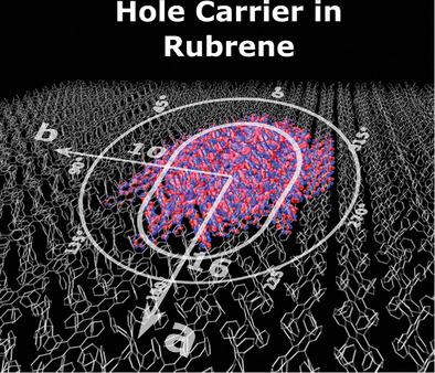
Progress in the design of high‐mobility organic semiconductors has been hampered by an incomplete fundamental understanding of the elusive charge carrier dynamics mediating electrical current in these materials. To address this problem, a novel fully atomistic non‐adiabatic molecular dynamics approach termed fragment orbital‐based surface hopping (FOB‐SH) that propagates the electron‐nuclear motion has been further improved and, for the first time, used to calculate the full 2D charge mobility tensor for the conductive planes of six structurally well characterized organic single crystals, in good agreement with available experimental data. The nature of the charge carrier in these materials is best described as a flickering polaron constantly changing shape and extensions under the influence of thermal disorder. Thermal intra‐band excitations from modestly delocalized band edge states (up to 5 nm or 10–20 molecules) to highly delocalized tail states (up to 10 nm or 40–60 molecules in the most conductive materials) give rise to short, ≈ 10 fs‐long bursts of the charge carrier wavefunction that drives the spatial displacement of the polaron, resulting in carrier diffusion and mobility. This study implies that key to the design of high‐mobility materials is a high density of strongly delocalized and thermally accessible tail states.
中文翻译:

延伸超过十纳米的闪烁极化子介导高迁移率有机晶体中的电荷传输
高迁移率有机半导体设计的进展因对在这些材料中介导电流的难以捉摸的电荷载流子动力学的不完整的基本理解而受到阻碍。为了解决这个问题,一种新的完全原子化的非绝热分子动力学方法被称为碎片轨道基表面跳变(FOB-SH),它可以传播电子核运动,并且已经得到了进一步改进,并且首次用于计算全电子六个结构良好表征的有机单晶的导电平面的二维电荷迁移率张量,与可用的实验数据高度吻合。这些材料中电荷载体的性质最好描述为闪烁的极化子,在热失调的影响下其形状和延伸不断变化。从适度离域的带边缘态(最多5 nm或10–20分子)到高度离域的尾态(在最导电的材料中高达10 nm或40–60分子)的带内热激发引起短路,≈10电荷载流子函数的fs长脉冲,驱动极化子的空间位移,导致载流子扩散和迁移。这项研究表明,高迁移率材料设计的关键是高密度的高度离域和热可接近的尾态。导致载流子扩散和迁移。这项研究表明,高迁移率材料设计的关键是高密度的高度离域和热可接近的尾态。导致载流子扩散和迁移。这项研究表明,高迁移率材料设计的关键是高密度的高度离域和热可接近的尾态。
更新日期:2020-07-06
中文翻译:
延伸超过十纳米的闪烁极化子介导高迁移率有机晶体中的电荷传输
高迁移率有机半导体设计的进展因对在这些材料中介导电流的难以捉摸的电荷载流子动力学的不完整的基本理解而受到阻碍。为了解决这个问题,一种新的完全原子化的非绝热分子动力学方法被称为碎片轨道基表面跳变(FOB-SH),它可以传播电子核运动,并且已经得到了进一步改进,并且首次用于计算全电子六个结构良好表征的有机单晶的导电平面的二维电荷迁移率张量,与可用的实验数据高度吻合。这些材料中电荷载体的性质最好描述为闪烁的极化子,在热失调的影响下其形状和延伸不断变化。从适度离域的带边缘态(最多5 nm或10–20分子)到高度离域的尾态(在最导电的材料中高达10 nm或40–60分子)的带内热激发引起短路,≈10电荷载流子函数的fs长脉冲,驱动极化子的空间位移,导致载流子扩散和迁移。这项研究表明,高迁移率材料设计的关键是高密度的高度离域和热可接近的尾态。导致载流子扩散和迁移。这项研究表明,高迁移率材料设计的关键是高密度的高度离域和热可接近的尾态。导致载流子扩散和迁移。这项研究表明,高迁移率材料设计的关键是高密度的高度离域和热可接近的尾态。


 京公网安备 11010802027423号