当前位置:
X-MOL 学术
›
ACS Appl. Electron. Mater.
›
论文详情
Our official English website, www.x-mol.net, welcomes your
feedback! (Note: you will need to create a separate account there.)
Dipolar Alignment in a Ferroelectric Dielectric Layer of FeFETs to Boost Charge Mobility and Nonvolatile Memory
ACS Applied Electronic Materials ( IF 4.3 ) Pub Date : 2020-09-20 , DOI: 10.1021/acsaelm.0c00549 Dhrubojyoti Roy, Partho Sarathi Gooh Pattader, Dipankar Bandyopadhyay, Mohua Chakraborty, Chia-Hsin Wang, Yaw-Wen Yang, Manabendra Mukherjee
ACS Applied Electronic Materials ( IF 4.3 ) Pub Date : 2020-09-20 , DOI: 10.1021/acsaelm.0c00549 Dhrubojyoti Roy, Partho Sarathi Gooh Pattader, Dipankar Bandyopadhyay, Mohua Chakraborty, Chia-Hsin Wang, Yaw-Wen Yang, Manabendra Mukherjee
|
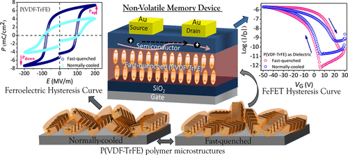
Influence of dipolar alignments of a ferroelectric poly-vinylidine fluoride trifluroethylene [P(VDF-TrFE)] thin film on the charge mobility and nonvolatile property of ferroelectric field-effect transistors (FeFETs) has been explored. The electrical properties of the ferroelectric microstructures can be tuned by adopting different cooling procedures after annealing the spin-coated ferroelectric polymer P(VDF-TrFE) substrates. For example, a higher degree of alignment of the C–F dipoles in the polymeric chains is observed along the substrate surface for the samples with fast quenching. The dielectric constant of the fast-quenched sample is found to be ∼10 at 1 kHz, while the same is found to be ∼8.5 when the rate of cooling is relatively slower. Furthermore, the fabrication of a metal–insulator–metal capacitor using the fast-quenched substrate leads to a high remnant polarization of Pr ∼ 5.5 ± 0.2 μC/cm2, as compared to that of the normally cooled sample to ∼2.7 ± 0.2 μC/cm2, at an applied field intensity of 200 MV/m. Emergence of such characteristics encouraged the use of P(VDF-TrFE) as a gate dielectric layer, which leads to improved nonvolatile characteristics of the device. The measured charge carrier mobility of FeFETs embedded with a fast-quenched ferroelectric polymer as a gate dielectric is found to be ∼3.4 × 10⁻² cm2 V–1 s–1, which is ∼35% higher than the normally cooled samples. The strongly correlated C–F dipoles in the fast-quenched ferroelectric layers lead to the reduction in width of the trap density of states near the semiconductor–dielectric interface. The XPS and UPS characterizations show the formation of a superior transport channel in the semiconductor near its dielectric interface when the fast-quenched polymer is used as the gate dielectric in the FeFETs.
中文翻译:

FeFET的铁电介质层中的偶极对准可提高电荷迁移率和非易失性存储器
研究了铁电聚偏氟乙烯三氟乙烯[P(VDF-TrFE)]薄膜的偶极取向对铁电场效应晶体管(FeFET)的电荷迁移率和非易失性的影响。在对旋涂的铁电聚合物P(VDF-TrFE)基板进行退火之后,可以通过采用不同的冷却程序来调整铁电微结构的电性能。例如,对于快速淬灭的样品,沿着基材表面观察到聚合物链中C-F偶极子的排列程度较高。快速淬火样品的介电常数在1 kHz时约为10,而在冷却速度相对较慢时,介电常数约为8.5。此外,P - [R〜5.5±0.2μC/厘米2相比于正常冷却的样品至~2.7±0.2μC/厘米,2,在200 MV / m的施加磁场强度。这种特性的出现鼓励使用P(VDF-TrFE)作为栅极介电层,从而提高了器件的非易失性。嵌入快速淬火铁电聚合物作为栅极电介质的FeFET的测得的载流子迁移率约为3.4×10 –2 cm 2 V –1 s –1比正常冷却的样品高约35%。快速淬灭的铁电层中强相关的C-F偶极子导致半导体-电介质界面附近的态陷阱密度的减小。XPS和UPS的特性表明,当快速淬灭的聚合物用作FeFET中的栅极电介质时,在其电介质界面附近的半导体中会形成一个优良的传输通道。
更新日期:2020-10-28
中文翻译:
FeFET的铁电介质层中的偶极对准可提高电荷迁移率和非易失性存储器
研究了铁电聚偏氟乙烯三氟乙烯[P(VDF-TrFE)]薄膜的偶极取向对铁电场效应晶体管(FeFET)的电荷迁移率和非易失性的影响。在对旋涂的铁电聚合物P(VDF-TrFE)基板进行退火之后,可以通过采用不同的冷却程序来调整铁电微结构的电性能。例如,对于快速淬灭的样品,沿着基材表面观察到聚合物链中C-F偶极子的排列程度较高。快速淬火样品的介电常数在1 kHz时约为10,而在冷却速度相对较慢时,介电常数约为8.5。此外,P - [R〜5.5±0.2μC/厘米2相比于正常冷却的样品至~2.7±0.2μC/厘米,2,在200 MV / m的施加磁场强度。这种特性的出现鼓励使用P(VDF-TrFE)作为栅极介电层,从而提高了器件的非易失性。嵌入快速淬火铁电聚合物作为栅极电介质的FeFET的测得的载流子迁移率约为3.4×10 –2 cm 2 V –1 s –1比正常冷却的样品高约35%。快速淬灭的铁电层中强相关的C-F偶极子导致半导体-电介质界面附近的态陷阱密度的减小。XPS和UPS的特性表明,当快速淬灭的聚合物用作FeFET中的栅极电介质时,在其电介质界面附近的半导体中会形成一个优良的传输通道。


 京公网安备 11010802027423号