当前位置:
X-MOL 学术
›
Adv. Mater. Interfaces
›
论文详情
Our official English website, www.x-mol.net, welcomes your
feedback! (Note: you will need to create a separate account there.)
Densely Arrayed Active Antennas Embedded in Vertical Nanoholes for Backside‐Illuminated Silicon‐Based Broadband Infrared Photodetection
Advanced Materials Interfaces ( IF 4.3 ) Pub Date : 2020-09-17 , DOI: 10.1002/admi.202001039 Shun Yasunaga 1, 2 , Hidetoshi Takahashi 3 , Tomoyuki Takahata 2 , Isao Shimoyama 4, 5 , Tetsuo Kan 1
Advanced Materials Interfaces ( IF 4.3 ) Pub Date : 2020-09-17 , DOI: 10.1002/admi.202001039 Shun Yasunaga 1, 2 , Hidetoshi Takahashi 3 , Tomoyuki Takahata 2 , Isao Shimoyama 4, 5 , Tetsuo Kan 1
Affiliation
|
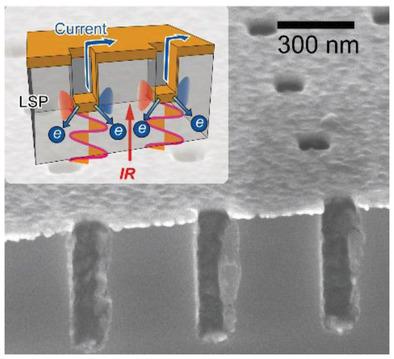
Plasmonic metal nanoantennas arrayed on silicon have attracted attention as silicon‐based sub‐bandgap infrared detectors. Localized surface plasmons induced on metal nanoblocks can provide a broadband responsivity, and the silicon‐based configuration offers the potential for complementary metal oxide semiconductor‐compatible infrared photodetectors. The responsivity of such devices, however, needs further improvement. In this report, a nanoantenna structure consisting of a nanoblock with electrical connection to it built in a narrow, vertical, and deep nanohole is presented, which generates a photocurrent in response to backside illumination. Inclined evaporative deposition of copper onto an array of nanoholes, 150 nm in diameter and 560 nm in depth, simultaneously forms nanoblocks and thin conductive films. The structure's effectiveness is demonstrated from the reflectance and responsivity to infrared laser illumination 1.1–1.8 µm in wavelength. When the periodicity of the nanoholes is 500 nm, a responsivity of 9.8 mA W−1 at 1.55 µm is obtained, which is sustained over a broad band. The responsivity–density relationship has a limitation between periodicities of 250 and 500 nm, possibly because of overlapped near fields around antennas and the resultant altered resonant mode. With its simple fabrication and efficient functionality, the nanoantenna structure contributes to the realization of silicon‐based infrared imaging.
中文翻译:

嵌入垂直纳米孔中的密集阵列有源天线,用于背面照明的硅基宽带红外光电检测
作为基于硅的亚带隙红外探测器,排列在硅上的等离子金属纳米天线引起了人们的关注。在金属纳米块上感应的局部表面等离子体激元可以提供宽带响应性,而基于硅的配置为互补金属氧化物半导体兼容的红外光电探测器提供了潜力。但是,这种设备的响应度需要进一步提高。在此报告中,提出了一种纳米天线结构,该结构由纳米块组成,该纳米块具有与之电连接的纳米块,该纳米块构建在一个狭窄的垂直垂直深纳米孔中,该纳米孔响应于背面照明而产生光电流。将铜倾斜蒸发沉积到直径为150 nm,深度为560 nm的纳米孔阵列上,同时形成纳米块和导电薄膜。结构' 从波长为1.1-1.8 µm的红外激光照射的反射率和响应度可以证明其有效性。当纳米孔的周期性为500 nm时,响应度为9.8 mA W获得了1.55 µm的-1,该信号在宽频带上保持不变。响应-密度关系在250和500 nm的周期之间有一个限制,这可能是由于天线周围的近场重叠以及由此导致的谐振模式改变所致。凭借其简单的制造和高效的功能性,纳米天线结构有助于实现基于硅的红外成像。
更新日期:2020-11-06
中文翻译:
嵌入垂直纳米孔中的密集阵列有源天线,用于背面照明的硅基宽带红外光电检测
作为基于硅的亚带隙红外探测器,排列在硅上的等离子金属纳米天线引起了人们的关注。在金属纳米块上感应的局部表面等离子体激元可以提供宽带响应性,而基于硅的配置为互补金属氧化物半导体兼容的红外光电探测器提供了潜力。但是,这种设备的响应度需要进一步提高。在此报告中,提出了一种纳米天线结构,该结构由纳米块组成,该纳米块具有与之电连接的纳米块,该纳米块构建在一个狭窄的垂直垂直深纳米孔中,该纳米孔响应于背面照明而产生光电流。将铜倾斜蒸发沉积到直径为150 nm,深度为560 nm的纳米孔阵列上,同时形成纳米块和导电薄膜。结构' 从波长为1.1-1.8 µm的红外激光照射的反射率和响应度可以证明其有效性。当纳米孔的周期性为500 nm时,响应度为9.8 mA W获得了1.55 µm的-1,该信号在宽频带上保持不变。响应-密度关系在250和500 nm的周期之间有一个限制,这可能是由于天线周围的近场重叠以及由此导致的谐振模式改变所致。凭借其简单的制造和高效的功能性,纳米天线结构有助于实现基于硅的红外成像。


 京公网安备 11010802027423号