当前位置:
X-MOL 学术
›
Phys. Status Solidi. Rapid Res. Lett.
›
论文详情
Our official English website, www.x-mol.net, welcomes your
feedback! (Note: you will need to create a separate account there.)
In‐plane Epitaxy of Bi2S3 Nanowire Arrays for Ultrasensitive NIR Photodetectors
Physica Status Solidi-Rapid Research Letters ( IF 2.5 ) Pub Date : 2020-09-16 , DOI: 10.1002/pssr.202000384 Xing Xu 1 , Chao Fan 1 , Yanguo Wang 2 , Zhuodong Qi 1 , Beibei Dai 1 , Haotian Jiang 1 , Shaowei Wang 3 , Qinglin Zhang 1
Physica Status Solidi-Rapid Research Letters ( IF 2.5 ) Pub Date : 2020-09-16 , DOI: 10.1002/pssr.202000384 Xing Xu 1 , Chao Fan 1 , Yanguo Wang 2 , Zhuodong Qi 1 , Beibei Dai 1 , Haotian Jiang 1 , Shaowei Wang 3 , Qinglin Zhang 1
Affiliation
|
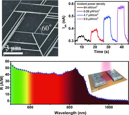
The direct growth of semiconductor nanowire (NW) arrays horizontally aligned on a substrate is critically important for the applications of NWs in electronic or optoelectronic devices at the circuit level. The strict requirement of lattice matching between a substrate and a material in the covalent epitaxy of crystals makes the wire arrays be grown on the substrates only with similar lattice parameters. Herein, a van der Waals epitaxy route is developed to realize the in‐plane growth of large‐scale Bi2S3 NW arrays on mica with a large lattice mismatch. The orthorhombic Bi2S3 NWs grow epitaxially with the axial direction of along the six symmetric directions of the mica. Transmission electron microscope measurements show that the epitaxial relationships are and along the length and width directions of the wires, respectively. More importantly, photodetectors based on Bi2S3 NWs show a wide photoresponse spectrum range from 500 to 980 nm. A high responsivity (5233 A W−1) and a specific detectivity (1.8 × 10¹² Jones) are achieved under 830 nm light irradiation with ultralow intensity (64 nW cm−2). In addition, the photodetectors exhibit high stability with at least 48 day storage in ambient atmosphere or with 1000 times bending.
中文翻译:

用于超灵敏NIR光电探测器的Bi2S3纳米线阵列的面内外延
水平排列在基板上的半导体纳米线(NW)阵列的直接生长对于NW在电路级的电子或光电设备中的应用至关重要。在晶体的共价外延中,基板与材料之间的晶格匹配的严格要求使得线阵列仅以相似的晶格参数在基板上生长。在本文中,发展了范德华外延路线,以实现大型Bi 2 S 3 NW阵列在具有大晶格失配的云母上的面内生长。斜方Bi 2 S 3 NWs沿轴向向外延生长。沿着云母的六个对称方向。透射电子显微镜测量表明外延关系是 和 分别沿着导线的长度和宽度方向。更重要的是,基于Bi 2 S 3 NW的光电探测器显示了从500到980 nm的宽光响应光谱范围。 在830nm的光和超低强度(64nW cm -2)下获得高响应度(5233A W -1)和比检测率(1.8×10 12 Jones )。此外,光电探测器在环境大气中至少存放48天或弯曲1000倍后表现出很高的稳定性。
更新日期:2020-11-02
中文翻译:
用于超灵敏NIR光电探测器的Bi2S3纳米线阵列的面内外延
水平排列在基板上的半导体纳米线(NW)阵列的直接生长对于NW在电路级的电子或光电设备中的应用至关重要。在晶体的共价外延中,基板与材料之间的晶格匹配的严格要求使得线阵列仅以相似的晶格参数在基板上生长。在本文中,发展了范德华外延路线,以实现大型Bi 2 S 3 NW阵列在具有大晶格失配的云母上的面内生长。斜方Bi 2 S 3 NWs沿轴向向外延生长。沿着云母的六个对称方向。透射电子显微镜测量表明外延关系是 和 分别沿着导线的长度和宽度方向。更重要的是,基于Bi 2 S 3 NW的光电探测器显示了从500到980 nm的宽光响应光谱范围。 在830nm的光和超低强度(64nW cm -2)下获得高响应度(5233A W -1)和比检测率(1.8×10 12 Jones )。此外,光电探测器在环境大气中至少存放48天或弯曲1000倍后表现出很高的稳定性。


 京公网安备 11010802027423号