当前位置:
X-MOL 学术
›
Adv. Mater.
›
论文详情
Our official English website, www.x-mol.net, welcomes your
feedback! (Note: you will need to create a separate account there.)
High-Throughput Growth of Wafer-Scale Monolayer Transition Metal Dichalcogenide via Vertical Ostwald Ripening.
Advanced Materials ( IF 27.4 ) Pub Date : 2020-09-16 , DOI: 10.1002/adma.202003542 Minsu Seol 1 , Min-Hyun Lee 1 , Haeryong Kim 1 , Keun Wook Shin 1 , Yeonchoo Cho 1 , Insu Jeon 1 , Myoungho Jeong 1 , Hyung-Ik Lee 1 , Jiwoong Park 2 , Hyeon-Jin Shin 1
Advanced Materials ( IF 27.4 ) Pub Date : 2020-09-16 , DOI: 10.1002/adma.202003542 Minsu Seol 1 , Min-Hyun Lee 1 , Haeryong Kim 1 , Keun Wook Shin 1 , Yeonchoo Cho 1 , Insu Jeon 1 , Myoungho Jeong 1 , Hyung-Ik Lee 1 , Jiwoong Park 2 , Hyeon-Jin Shin 1
Affiliation
|
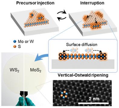
For practical device applications, monolayer transition metal dichalcogenide (TMD) films must meet key industry needs for batch processing, including the high‐throughput, large‐scale production of high‐quality, spatially uniform materials, and reliable integration into devices. Here, high‐throughput growth, completed in 12 min, of 6‐inch wafer‐scale monolayer MoS2 and WS2 is reported, which is directly compatible with scalable batch processing and device integration. Specifically, a pulsed metal–organic chemical vapor deposition process is developed, where periodic interruption of the precursor supply drives vertical Ostwald ripening, which prevents secondary nucleation despite high precursor concentrations. The as‐grown TMD films show excellent spatial homogeneity and well‐stitched grain boundaries, enabling facile transfer to various target substrates without degradation. Using these films, batch fabrication of high‐performance field‐effect transistor (FET) arrays in wafer‐scale is demonstrated, and the FETs show remarkable uniformity. The high‐throughput production and wafer‐scale automatable transfer will facilitate the integration of TMDs into Si‐complementary metal‐oxide‐semiconductor platforms.
中文翻译:

晶圆级单层过渡金属二硫属化物通过垂直奥斯特瓦尔德熟化的高通量生长。
对于实际的设备应用,单层过渡金属二硫化碳(TMD)膜必须满足批量处理的关键行业需求,包括高通量,大规模生产高质量,空间均匀的材料以及可靠地集成到设备中。此处,在12分钟内完成了6英寸晶圆级单层MoS 2和WS 2的高通量增长报告,它与可伸缩批处理和设备集成直接兼容。特别是,开发了脉冲式金属有机化学气相沉积工艺,该工艺中周期性中断前驱物供应,从而导致垂直奥斯特瓦尔德熟化,尽管前驱物浓度很高,但仍可防止二次成核。刚成膜的TMD薄膜具有出色的空间均匀性和良好缝合的晶界,可轻松转移到各种目标基材而不会降解。使用这些薄膜,演示了晶圆级高性能场效应晶体管(FET)阵列的批量制造,并且FET显示出显着的均匀性。高通量的生产和晶圆规模的自动转移将促进TMD集成到硅互补金属氧化物半导体平台中。
更新日期:2020-10-20
中文翻译:
晶圆级单层过渡金属二硫属化物通过垂直奥斯特瓦尔德熟化的高通量生长。
对于实际的设备应用,单层过渡金属二硫化碳(TMD)膜必须满足批量处理的关键行业需求,包括高通量,大规模生产高质量,空间均匀的材料以及可靠地集成到设备中。此处,在12分钟内完成了6英寸晶圆级单层MoS 2和WS 2的高通量增长报告,它与可伸缩批处理和设备集成直接兼容。特别是,开发了脉冲式金属有机化学气相沉积工艺,该工艺中周期性中断前驱物供应,从而导致垂直奥斯特瓦尔德熟化,尽管前驱物浓度很高,但仍可防止二次成核。刚成膜的TMD薄膜具有出色的空间均匀性和良好缝合的晶界,可轻松转移到各种目标基材而不会降解。使用这些薄膜,演示了晶圆级高性能场效应晶体管(FET)阵列的批量制造,并且FET显示出显着的均匀性。高通量的生产和晶圆规模的自动转移将促进TMD集成到硅互补金属氧化物半导体平台中。


 京公网安备 11010802027423号