Surface & Coatings Technology ( IF 5.4 ) Pub Date : 2020-09-16 , DOI: 10.1016/j.surfcoat.2020.126414 Liangge Xu , Lili He , Lei Yang , Zhibo Zhang , Shuai Guo , Zhenhuai Yang , Peng Wang , Fangjuan Geng , Gang Gao , Chunqiang Sun , Victor Ralchenko , Jiaqi Zhu
|
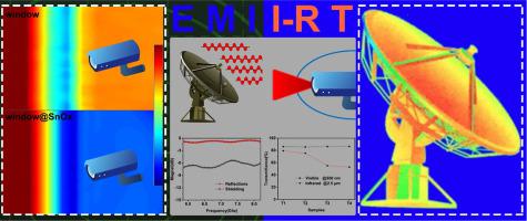
The performance of atomic layer deposition films is mainly limited by precursor residues, low crystallinity and densities due to low deposition temperatures. Here, we used atomic layer deposition to deposit tin oxide thin films at a relatively low temperature of 250 °C. At this temperature, the change in the valence of Sn due to precursor residue is eliminated by layer-by-layer Ar plasma treatment, and the crystallinity of the films is improved. The effects of Ar plasma treatment power and Ar treatment time on the structural and optoelectronic properties were investigated. It was found that Ar plasma treatment time more significantly affects the surface morphology and the optical and electrical properties of the film. The film is transparent to both visible and near-infrared light over a wide range of wavelengths from 400 nm to at least 5000 nm. The film resistivity can be as low as 1.117 × 10⁻³ Ω·cm. The film has a relatively low level of residual stress due to the fact that there is no need to improve the crystallinity of the film by conventional high temperature annealing. On the basis of the high transparency and high conductivity of the SnOx films with layer by layer Ar plasma treatment in situ, the films can be applied as electromagnetic shielding windows for photodetectors.
中文翻译:
进行等离子体处理以适应等离子体增强原子层沉积SnOx红外透明导电薄膜的生长和光电性能
原子层沉积膜的性能主要受前驱物残留,结晶度低和沉积温度低导致的密度限制。在这里,我们使用原子层沉积在相对较低的250°C温度下沉积氧化锡薄膜。在该温度下,通过逐层Ar等离子体处理消除了由于前体残渣引起的Sn的价态变化,并且提高了膜的结晶性。研究了氩等离子体处理能力和时间对结构和光电性能的影响。发现氩等离子体处理时间更显着地影响膜的表面形态以及光学和电学性质。该膜对在400 nm至至少5000 nm的宽波长范围内的可见光和近红外光均透明。-3 Ω·cm以下。由于不需要通过常规的高温退火来提高膜的结晶度的事实,膜具有相对较低的残余应力水平。基于原位逐层Ar等离子处理的SnOx薄膜的高透明性和高导电性,这些薄膜可以用作光电探测器的电磁屏蔽窗口。


 京公网安备 11010802027423号