当前位置:
X-MOL 学术
›
ACS Photonics
›
论文详情
Our official English website, www.x-mol.net, welcomes your
feedback! (Note: you will need to create a separate account there.)
Photoexcited Free Carrier Dynamics in Bi2Se3, (Bi0.75In0.25)2Se3, and (Bi0.50In0.50)2Se3: From Topological to Band Insulator
ACS Photonics ( IF 6.5 ) Pub Date : 2020-09-14 , DOI: 10.1021/acsphotonics.0c00928 Teng Shi 1 , Kateryna Kushnir 1 , Zhengtianye Wang 2 , Stephanie Law 2 , Lyubov V. Titova 1
ACS Photonics ( IF 6.5 ) Pub Date : 2020-09-14 , DOI: 10.1021/acsphotonics.0c00928 Teng Shi 1 , Kateryna Kushnir 1 , Zhengtianye Wang 2 , Stephanie Law 2 , Lyubov V. Titova 1
Affiliation
|
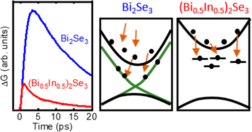
Replacing some Bi with In in Bi2Se3 transforms it from a topological insulator to a band insulator. Here, we have used time-resolved terahertz spectroscopy to investigate photoexcited carrier dynamics in (Bi1–xInx)2Se3 films with indium concentration x = 0%, 25%, and 50%. In Bi2Se3, optically excited carriers scatter from the bulk conduction band states into high mobility topological surface states within picoseconds after excitation. We demonstrate that a second set of Dirac surface states, located ∼1.5–1.8 eV above the conduction band minimum and accessible to carriers excited by 3.1 eV pulses, is characterized by a higher mobility than the surface states within the band gap that dominate equilibrium conductivity. In (Bi0.75In0.25)2Se3 and (Bi0.50In0.50)2Se3, which are insulating without photoexcitation, the dynamics of photoexcited free carriers are affected by the twin domain boundaries and are sensitive to the disorder introduced by indium substitution. Transient conductivity rise time, as well as the mobility and lifetime of the photoexcited carriers in (Bi1–xInx)2Se3 films, can be tuned by the indium content, enabling tailoring of band insulators that have the desired optoelectronic properties and are fully structurally compatible with the topological insulator Bi2Se3 for applications in high-speed photonic devices based on topological insulator/band insulator heterostructures.
中文翻译:

Bi 2 Se 3,(Bi 0.75 In 0.25)2 Se 3和(Bi 0.50 In 0.50)2 Se 3中的光激发自由载流子动力学:从拓扑到带绝缘子
用Bi 2 Se 3中的In代替某些Bi会将其从拓扑绝缘体转变为带状绝缘体。在这里,我们使用时间分辨太赫兹光谱研究了铟浓度x = 0%,25%和50%的(Bi 1– x In x)2 Se 3薄膜中的光激发载流子动力学。在Bi 2 Se 3中在激发后的皮秒内,光激发载流子从体导带状态散射到高迁移率拓扑表面状态。我们证明了第二组狄拉克表面态,位于导带最小值以上约1.5-1.8 eV,并且可被3.1 eV脉冲激发的载流子访问,其迁移率高于带隙内支配平衡电导率的表面态。 。In(Bi 0.75 In 0.25)2 Se 3和(Bi 0.50 In 0.50)2 Se 3在没有光激发的情况下是绝缘的,光激发自由载流子的动力学受孪晶域边界的影响,并对铟取代引起的无序敏感。瞬态电导率的上升时间,以及(Bi 1– x In x)2 Se 3膜中光激发载流子的迁移率和寿命,可以通过铟含量来调节,从而能够定制具有所需光电特性和与拓扑绝缘体Bi 2 Se 3在结构上完全兼容,可用于基于拓扑绝缘体/带状绝缘体异质结构的高速光子器件。
更新日期:2020-10-21
中文翻译:
Bi 2 Se 3,(Bi 0.75 In 0.25)2 Se 3和(Bi 0.50 In 0.50)2 Se 3中的光激发自由载流子动力学:从拓扑到带绝缘子
用Bi 2 Se 3中的In代替某些Bi会将其从拓扑绝缘体转变为带状绝缘体。在这里,我们使用时间分辨太赫兹光谱研究了铟浓度x = 0%,25%和50%的(Bi 1– x In x)2 Se 3薄膜中的光激发载流子动力学。在Bi 2 Se 3中在激发后的皮秒内,光激发载流子从体导带状态散射到高迁移率拓扑表面状态。我们证明了第二组狄拉克表面态,位于导带最小值以上约1.5-1.8 eV,并且可被3.1 eV脉冲激发的载流子访问,其迁移率高于带隙内支配平衡电导率的表面态。 。In(Bi 0.75 In 0.25)2 Se 3和(Bi 0.50 In 0.50)2 Se 3在没有光激发的情况下是绝缘的,光激发自由载流子的动力学受孪晶域边界的影响,并对铟取代引起的无序敏感。瞬态电导率的上升时间,以及(Bi 1– x In x)2 Se 3膜中光激发载流子的迁移率和寿命,可以通过铟含量来调节,从而能够定制具有所需光电特性和与拓扑绝缘体Bi 2 Se 3在结构上完全兼容,可用于基于拓扑绝缘体/带状绝缘体异质结构的高速光子器件。


 京公网安备 11010802027423号