当前位置:
X-MOL 学术
›
ACS Appl. Nano Mater.
›
论文详情
Our official English website, www.x-mol.net, welcomes your feedback! (Note: you will need to create a separate account there.)
Large-Scale Vertical 1T′/2H MoTe2 Nanosheet-Based Heterostructures for Low Contact Resistance Transistors
ACS Applied Nano Materials ( IF 5.9 ) Pub Date : 2020-09-11 , DOI: 10.1021/acsanm.0c02302 Shiqi Yang 1, 2 , Xiaolong Xu 1 , Wanjin Xu 1 , Bo Han 3 , Zhengping Ding 3 , Pingfan Gu 1 , Peng Gao 3, 4, 5 , Yu Ye 1, 4, 6
ACS Applied Nano Materials ( IF 5.9 ) Pub Date : 2020-09-11 , DOI: 10.1021/acsanm.0c02302 Shiqi Yang 1, 2 , Xiaolong Xu 1 , Wanjin Xu 1 , Bo Han 3 , Zhengping Ding 3 , Pingfan Gu 1 , Peng Gao 3, 4, 5 , Yu Ye 1, 4, 6
Affiliation
|
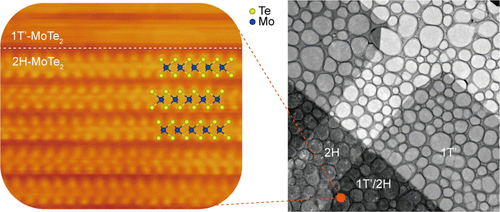
Because of atomic thickness and non-zero band gap, two-dimensional (2D) transition-metal dichalcogenides (TMDCs) have become promising candidates for post-silicon nanoelectronic materials. In the process of realizing 2D electronic devices for scaling down modern integrated circuitry, contact engineering suitable for large-scale manufacturing is crucial, but it remains elusive. Here, we demonstrated the large-scale chemical assembly of van der Waals heterostructures, with metallic 1T′-MoTe2 on top of semiconducting 2H-MoTe2, via a spatial-controlled phase-engineered growth method. Based on the heterophase structure, a large-scale field-effect transistor (FET) array was fabricated, in which 1T′-MoTe2 was used as the contact electrode and 2H-MoTe2 was used as the semiconducting channel. The vertical nanosheet-based heterophase FET exhibits ohmic contact behavior with distinctively low contact resistance. A total of 120 FETs were measured, and the measured average field-effect mobility was as high as 15 cm2 V–1 s–1 (comparable to that of exfoliated single-crystalline 2H-MoTe2). The superior electrical properties are attributed to the atomic clean interface that leads to an ideal contact between top 1T′- and bottom 2H-MoTe2. This spatially controlled large-scale chemical assembly of vertical 2D metal–semiconductor heterostructures with low contact resistance provides a new route toward the practical application of high-performance electronic and optoelectronic devices based on the atomically thin TMDCs.
中文翻译:

用于低接触电阻晶体管的大规模垂直1T′/ 2H MoTe 2纳米片基异质结构
由于原子厚度和非零带隙,二维(2D)过渡金属二卤化金属(TMDC)已成为后硅纳米电子材料的有希望的候选者。在实现用于缩小现代集成电路规模的2D电子设备的过程中,适合大规模生产的接触工程至关重要,但仍然难以捉摸。在这里,我们通过空间控制的相工程生长方法,证明了范德华异质结构的大规模化学组装,其中金属1T'-MoTe 2位于半导体2H-MoTe 2的顶部。基于异相结构,制备了大规模场效应晶体管(FET)阵列,其中1T'-MoTe 2被用作接触电极,而2H-MoTe 2被用作接触电极。被用作半导体通道。垂直的基于纳米片的异相FET表现出欧姆接触行为,且接触电阻极低。总共测量了120个FET,测得的平均场效应迁移率高达15 cm 2 V –1 s –1(与片状单晶2H-MoTe 2相比)。优异的电性能归因于原子清洁界面,可在顶部1T'-和底部2H-MoTe 2之间实现理想的接触。 具有低接触电阻的垂直二维金属-半导体异质结构的空间控制大规模化学组装为基于原子薄TMDC的高性能电子和光电器件的实际应用提供了一条新途径。
更新日期:2020-10-25
中文翻译:
用于低接触电阻晶体管的大规模垂直1T′/ 2H MoTe 2纳米片基异质结构
由于原子厚度和非零带隙,二维(2D)过渡金属二卤化金属(TMDC)已成为后硅纳米电子材料的有希望的候选者。在实现用于缩小现代集成电路规模的2D电子设备的过程中,适合大规模生产的接触工程至关重要,但仍然难以捉摸。在这里,我们通过空间控制的相工程生长方法,证明了范德华异质结构的大规模化学组装,其中金属1T'-MoTe 2位于半导体2H-MoTe 2的顶部。基于异相结构,制备了大规模场效应晶体管(FET)阵列,其中1T'-MoTe 2被用作接触电极,而2H-MoTe 2被用作接触电极。被用作半导体通道。垂直的基于纳米片的异相FET表现出欧姆接触行为,且接触电阻极低。总共测量了120个FET,测得的平均场效应迁移率高达15 cm 2 V –1 s –1(与片状单晶2H-MoTe 2相比)。优异的电性能归因于原子清洁界面,可在顶部1T'-和底部2H-MoTe 2之间实现理想的接触。 具有低接触电阻的垂直二维金属-半导体异质结构的空间控制大规模化学组装为基于原子薄TMDC的高性能电子和光电器件的实际应用提供了一条新途径。


 京公网安备 11010802027423号