当前位置:
X-MOL 学术
›
Phys. Status Solidi A
›
论文详情
Our official English website, www.x-mol.net, welcomes your
feedback! (Note: you will need to create a separate account there.)
Monolithic Integrated AlGaN/GaN Power Converter Topologies on High‐Voltage AlN/GaN Superlattice Buffer
Physica Status Solidi (A) - Applications and Materials Science Pub Date : 2020-09-10 , DOI: 10.1002/pssa.202000404 Stefan Moench 1 , Stefan Müller 1 , Richard Reiner 1 , Patrick Waltereit 1 , Heiko Czap 1 , Michael Basler 1 , Jan Hückelheim 2 , Lutz Kirste 1 , Ingmar Kallfass 2 , Rüdiger Quay 1 , Oliver Ambacher 1
Physica Status Solidi (A) - Applications and Materials Science Pub Date : 2020-09-10 , DOI: 10.1002/pssa.202000404 Stefan Moench 1 , Stefan Müller 1 , Richard Reiner 1 , Patrick Waltereit 1 , Heiko Czap 1 , Michael Basler 1 , Jan Hückelheim 2 , Lutz Kirste 1 , Ingmar Kallfass 2 , Rüdiger Quay 1 , Oliver Ambacher 1
Affiliation
|
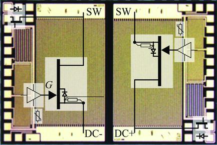
A high‐voltage AlN/GaN superlattice (SL) buffer for monolithic AlGaN/GaN power circuits is experimentally compared with a step‐graded AlGaN/GaN buffer. The SL as part of a 5.1 μm epitaxial stack withstands over 1.3 kV. Although the step‐graded buffer is sufficient for low‐side circuits, the operation voltage of monolithic topologies such as a half‐bridge is limited: static negative back gating at −200 V depletes the lateral channel completely. Asymmetrical buffer leakage at a positive substrate voltage of +250 V limits the operation voltage further. The SL buffer mitigates both effects: a negative substrate voltage of −200 V reduced the lateral channel current only by 25%. However, this condition is not required for half‐bridge operation on the SL, because low symmetrical vertical buffer leakage at substrate voltages of ±500 V allows operation of power topologies with positive substrate bias. High‐electron‐mobility transistors (HEMTs) on the graded buffer show excessive threshold voltage shift at negative substrate bias. On the SL buffer, the threshold voltage is shifted only +1 V from negative substrate biases, which allows monolithic high‐voltage power topology operation. 98.8% efficient operation of a 6 × 4 mm2 GaN‐on‐Si power integrated circuit with a monolithic half bridge, freewheeling diodes, and drivers is demonstrated on the SL.
中文翻译:

高压AlN / GaN超晶格缓冲器上的单片集成式AlGaN / GaN功率转换器拓扑
实验将用于单片式AlGaN / GaN电源电路的高压AlN / GaN超晶格(SL)缓冲器与逐步分级的AlGaN / GaN缓冲器进行了比较。作为5.1μm外延堆叠的一部分的SL可以承受1.3 kV以上的电压。尽管阶跃式缓冲器足以满足低端电路的需求,但单片拓扑(例如半桥)的工作电压仍然受到限制:−200 V的静态负向反向门控会完全耗尽横向通道。正基板电压为+250 V时,非对称缓冲器泄漏会进一步限制工作电压。SL缓冲器可减轻这两种影响:-200 V的负衬底电压仅将横向沟道电流降低了25%。但是,SL上的半桥操作不需要此条件,因为在±500 V的基板电压下,对称缓冲器的垂直泄漏很低,因此可以使电源拓扑在正的基板偏置下工作。渐变缓冲器上的高电子迁移率晶体管(HEMT)在负衬底偏置下显示出过高的阈值电压偏移。在SL缓冲器上,阈值电压仅从负衬底偏置偏移+1 V,从而允许单片高压电源拓扑操作。6×4毫米的效率为98.8%2在SL上展示了具有单片半桥,续流二极管和驱动器的GaN-on-Si电源集成电路。
更新日期:2020-09-10
中文翻译:
高压AlN / GaN超晶格缓冲器上的单片集成式AlGaN / GaN功率转换器拓扑
实验将用于单片式AlGaN / GaN电源电路的高压AlN / GaN超晶格(SL)缓冲器与逐步分级的AlGaN / GaN缓冲器进行了比较。作为5.1μm外延堆叠的一部分的SL可以承受1.3 kV以上的电压。尽管阶跃式缓冲器足以满足低端电路的需求,但单片拓扑(例如半桥)的工作电压仍然受到限制:−200 V的静态负向反向门控会完全耗尽横向通道。正基板电压为+250 V时,非对称缓冲器泄漏会进一步限制工作电压。SL缓冲器可减轻这两种影响:-200 V的负衬底电压仅将横向沟道电流降低了25%。但是,SL上的半桥操作不需要此条件,因为在±500 V的基板电压下,对称缓冲器的垂直泄漏很低,因此可以使电源拓扑在正的基板偏置下工作。渐变缓冲器上的高电子迁移率晶体管(HEMT)在负衬底偏置下显示出过高的阈值电压偏移。在SL缓冲器上,阈值电压仅从负衬底偏置偏移+1 V,从而允许单片高压电源拓扑操作。6×4毫米的效率为98.8%2在SL上展示了具有单片半桥,续流二极管和驱动器的GaN-on-Si电源集成电路。


 京公网安备 11010802027423号