当前位置:
X-MOL 学术
›
Adv. Electron. Mater.
›
论文详情
Our official English website, www.x-mol.net, welcomes your
feedback! (Note: you will need to create a separate account there.)
Prospects of Terahertz Transistors with the Topological Semimetal Cadmium Arsenide
Advanced Electronic Materials ( IF 5.3 ) Pub Date : 2020-09-11 , DOI: 10.1002/aelm.202000676 Omor F. Shoron 1 , Manik Goyal 1 , Binghao Guo 1 , David A. Kealhofer 2 , Timo Schumann 1 , Susanne Stemmer 1
Advanced Electronic Materials ( IF 5.3 ) Pub Date : 2020-09-11 , DOI: 10.1002/aelm.202000676 Omor F. Shoron 1 , Manik Goyal 1 , Binghao Guo 1 , David A. Kealhofer 2 , Timo Schumann 1 , Susanne Stemmer 1
Affiliation
|
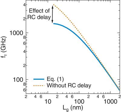
Electronic devices that operate at terahertz frequencies will require new materials that exhibit higher carrier velocities than traditional semiconductors. Calculations show that cadmium arsenide, a 3D topological (Dirac) semimetal, is an excellent candidate for field effect transistors that operate at frequencies above 1 THz. Moreover, such transistors have unique advantages that are enabled by the properties of Dirac electrons. These include predictions of an unprecedented linearity of the transconductance and cutoff frequencies over a large operating range and cutoff frequencies that remain above 1 THz at carrier densities as low as 1011 cm−2. The calculations are underpinned by measurements of devices with cadmium arsenide channels. Extremely low contact resistances (<2 × 10⁻⁹ Ω cm2), high electron velocities (>7 × 10⁵ m s−1), and unprecedentedly large current densities (up to 10 A mm−1) are demonstrated. Current modulation (>50%) and transconductance already achieved in the early transistors show the potential for large (>10 ×) improvements by reducing interface trap densities. The results demonstrate the significant potential of topological semimetals for high‐speed transistors operating in the THz regime and open up new opportunities for next‐generation RF circuits.
中文翻译:

拓扑半金属砷化镉太赫兹晶体管的前景
以太赫兹频率工作的电子设备将需要比传统半导体具有更高载流子速度的新材料。计算表明,砷化镉是一种3D拓扑(狄拉克(Dirac))半金属,是工作于1 THz以上频率的场效应晶体管的极佳候选者。此外,这样的晶体管具有由狄拉克电子的特性实现的独特优点。这些包括在大工作范围内跨导和截止频率的空前线性的预测,以及在低至10 11 cm -2的载流子密度下截止频率保持在1 THz以上的截止频率。通过对具有砷化镉通道的设备进行测量来支持计算。极低的接触电阻(<2×10⁻⁹ Ω厘米2),高电子速度(> 7×10 5毫秒-1),和空前巨大的电流密度(最多10个甲毫米-1)被证实。早期晶体管中已经实现的电流调制(> 50%)和跨导显示出通过降低界面陷阱密度来实现大幅度改进(> 10×)的潜力。结果表明,拓扑半金属对于以太赫兹频率运行的高速晶体管具有巨大的潜力,并为下一代射频电路开辟了新的机遇。
更新日期:2020-10-11
中文翻译:
拓扑半金属砷化镉太赫兹晶体管的前景
以太赫兹频率工作的电子设备将需要比传统半导体具有更高载流子速度的新材料。计算表明,砷化镉是一种3D拓扑(狄拉克(Dirac))半金属,是工作于1 THz以上频率的场效应晶体管的极佳候选者。此外,这样的晶体管具有由狄拉克电子的特性实现的独特优点。这些包括在大工作范围内跨导和截止频率的空前线性的预测,以及在低至10 11 cm -2的载流子密度下截止频率保持在1 THz以上的截止频率。通过对具有砷化镉通道的设备进行测量来支持计算。极低的接触电阻(<2×10⁻⁹ Ω厘米2),高电子速度(> 7×10 5毫秒-1),和空前巨大的电流密度(最多10个甲毫米-1)被证实。早期晶体管中已经实现的电流调制(> 50%)和跨导显示出通过降低界面陷阱密度来实现大幅度改进(> 10×)的潜力。结果表明,拓扑半金属对于以太赫兹频率运行的高速晶体管具有巨大的潜力,并为下一代射频电路开辟了新的机遇。


 京公网安备 11010802027423号