Journal of Manufacturing Processes ( IF 6.1 ) Pub Date : 2020-09-11 , DOI: 10.1016/j.jmapro.2020.08.050 Fumihiro Inoue , Arnita Podpod , Lan Peng , Alain Phommahaxay , Kenneth June Rebibis , Akira Uedono , Eric Beyne
|
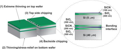
Direct wafer bonding is getting a standard and essential process in high density 3D integration devices. In this study, we investigated impact of direct bonding interface and extremely thinned Si on dicing and thinning processes. By comparing single wafer and direct bonded wafer having extreme thinned Si on top, bigger frontside chippings are observed after dicing for the case of direct bonded wafer. However, cross-sectional images unveil that the initiated point of the chipping is at the interface between SiCN and SiO2, not at the bonding interface. It indicates that direct bonding interface and 5 μm Si are not the root-cause of the chippings. For the backside thinning process, comprehensive analysis including atomic scale vacancy measurement/observation and macro level roughness/morphology analysis are executed. The major impact on die strength was given by macro level roughness. Despite having bigger chipping on bonded wafer, higher die strength is obtained from bonded wafer. It might be due to the stress buffering caused by bonding interface.
中文翻译:
通过在直接键合的硅片上切块和减薄的形态表征和机械性能
在高密度3D集成设备中,直接晶圆键合正在成为一种标准且必不可少的工艺。在这项研究中,我们研究了直接键合界面和极薄的硅对切割和减薄工艺的影响。通过比较单晶片和在顶部具有极薄的Si的直接粘合晶片,在切割后对于直接粘合晶片的情况观察到较大的正面碎裂。然而,横截面图像揭示了切屑的起始点位于SiCN和SiO 2之间的界面,而不是在绑定界面。这表明直接键合界面和5μmSi并不是碎屑的根本原因。对于背面薄化工艺,执行了包括原子尺度空位测量/观察和宏观水平粗糙度/形态分析在内的综合分析。对模具强度的主要影响是宏观粗糙度。尽管在键合晶片上有较大的缺口,但从键合晶片可获得更高的芯片强度。这可能是由于粘结界面引起的应力缓冲。


 京公网安备 11010802027423号