当前位置:
X-MOL 学术
›
ACS Appl. Mater. Interfaces
›
论文详情
Our official English website, www.x-mol.net, welcomes your
feedback! (Note: you will need to create a separate account there.)
Thermal Transport across Ion-Cut Monocrystalline β-Ga2O3 Thin Films and Bonded β-Ga2O3-SiC Interfaces.
ACS Applied Materials & Interfaces ( IF 8.3 ) Pub Date : 2020-09-10 , DOI: 10.1021/acsami.0c11672 Zhe Cheng 1 , Fengwen Mu 2, 3 , Tiangui You 4 , Wenhui Xu 4 , Jingjing Shi 1 , Michael E Liao 5 , Yekan Wang 5 , Kenny Huynh 5 , Tadatomo Suga 3 , Mark S Goorsky 5 , Xin Ou 4 , Samuel Graham 1, 6
ACS Applied Materials & Interfaces ( IF 8.3 ) Pub Date : 2020-09-10 , DOI: 10.1021/acsami.0c11672 Zhe Cheng 1 , Fengwen Mu 2, 3 , Tiangui You 4 , Wenhui Xu 4 , Jingjing Shi 1 , Michael E Liao 5 , Yekan Wang 5 , Kenny Huynh 5 , Tadatomo Suga 3 , Mark S Goorsky 5 , Xin Ou 4 , Samuel Graham 1, 6
Affiliation
|
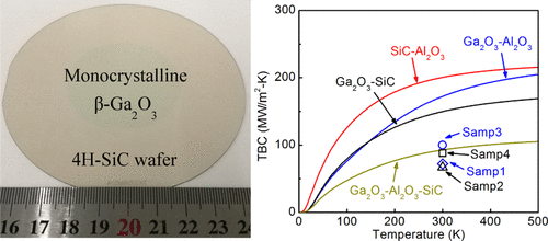
The ultrawide band gap, high breakdown electric field, and large-area affordable substrates make β-Ga2O3 promising for applications of next-generation power electronics, while its thermal conductivity is at least 1 order of magnitude lower than other wide/ultrawide band gap semiconductors. To avoid the degradation of device performance and reliability induced by the localized Joule-heating, proper thermal management strategies are essential, especially for high-power high-frequency applications. This work reports a scalable thermal management strategy to heterogeneously integrate wafer-scale monocrystalline β-Ga2O3 thin films on high thermal conductivity SiC substrates by the ion-cutting technique and room-temperature surface-activated bonding technique. The thermal boundary conductance (TBC) of the β-Ga2O3–SiC interfaces and thermal conductivity of the β-Ga2O3 thin films were measured by time-domain thermoreflectance to evaluate the effects of interlayer thickness and thermal annealing. Materials characterizations were performed to understand the mechanisms of thermal transport in these structures. The results show that the β-Ga2O3–SiC TBC values are reasonably high and increase with decreasing interlayer thickness. The β-Ga2O3 thermal conductivity increases more than twice after annealing at 800 °C because of the removal of implantation-induced strain in the films. A Callaway model is built to understand the measured thermal conductivity. Small spot-to-spot variations of both TBC and Ga2O3 thermal conductivity confirm the uniformity and high quality of the bonding and exfoliation. Our work paves the way for thermal management of power electronics and provides a platform for β-Ga2O3-related semiconductor devices with excellent thermal dissipation.
中文翻译:

跨离子切割单晶β-Ga2O3薄膜和键合的β-Ga2O3-SiC界面的热传输。
超宽带隙,高击穿电场,和大面积的经济的承印物使的β-Ga 2 ö 3希望用于下一代功率电子器件的应用,同时其热传导率是大小中的至少1个数量比其他宽/超宽降低带隙半导体。为了避免局部焦耳加热引起的器件性能和可靠性下降,正确的热管理策略至关重要,特别是对于大功率高频应用。这项工作报告一个可伸缩的热管理策略,非均相整合晶片规模单晶的β-Ga 2 ö 3通过离子切割技术和室温表面活化键合技术在高导热率SiC衬底上形成薄膜。所述的β-Ga的热边界电导(TBC)2 ö 3 -SiC界面和β-Ga中的热导率2 ö 3薄膜通过时域热反射测量来评价中间层厚度和热退火的效果。进行材料表征以了解这些结构中的热传递机理。结果表明,所述的β-Ga 2 ö 3个-SiC TBC值是相当高的,并与减小中间层的厚度增加。所述的β-Ga 2 ö 3在800°C退火后,热导率增加了两倍以上,这是因为消除了薄膜中注入引起的应变。建立了Callaway模型以了解测得的热导率。TBC和Ga 2 O 3导热系数的点到点变化很小,证实了键合和剥离的均匀性和高质量。我们的工作铺平了功率电子器件的热管理的方法,并提供了的β-Ga的平台2 ö 3具有优良的热耗散-相关的半导体器件。
更新日期:2020-10-07
中文翻译:
跨离子切割单晶β-Ga2O3薄膜和键合的β-Ga2O3-SiC界面的热传输。
超宽带隙,高击穿电场,和大面积的经济的承印物使的β-Ga 2 ö 3希望用于下一代功率电子器件的应用,同时其热传导率是大小中的至少1个数量比其他宽/超宽降低带隙半导体。为了避免局部焦耳加热引起的器件性能和可靠性下降,正确的热管理策略至关重要,特别是对于大功率高频应用。这项工作报告一个可伸缩的热管理策略,非均相整合晶片规模单晶的β-Ga 2 ö 3通过离子切割技术和室温表面活化键合技术在高导热率SiC衬底上形成薄膜。所述的β-Ga的热边界电导(TBC)2 ö 3 -SiC界面和β-Ga中的热导率2 ö 3薄膜通过时域热反射测量来评价中间层厚度和热退火的效果。进行材料表征以了解这些结构中的热传递机理。结果表明,所述的β-Ga 2 ö 3个-SiC TBC值是相当高的,并与减小中间层的厚度增加。所述的β-Ga 2 ö 3在800°C退火后,热导率增加了两倍以上,这是因为消除了薄膜中注入引起的应变。建立了Callaway模型以了解测得的热导率。TBC和Ga 2 O 3导热系数的点到点变化很小,证实了键合和剥离的均匀性和高质量。我们的工作铺平了功率电子器件的热管理的方法,并提供了的β-Ga的平台2 ö 3具有优良的热耗散-相关的半导体器件。


 京公网安备 11010802027423号