当前位置:
X-MOL 学术
›
ACS Appl. Nano Mater.
›
论文详情
Our official English website, www.x-mol.net, welcomes your
feedback! (Note: you will need to create a separate account there.)
Monolayer Graphene Grown on Nanoscale Pt Films Deposited on TiO2 Substrates for Micro- and Nanoelectromechanical Systems
ACS Applied Nano Materials ( IF 5.3 ) Pub Date : 2020-09-09 , DOI: 10.1021/acsanm.0c01839 Joon Hyong Cho 1 , Yoonho Seo 2 , Andrei Dolocan 3 , Neal A. Hall 2 , Michael A. Cullinan 1
ACS Applied Nano Materials ( IF 5.3 ) Pub Date : 2020-09-09 , DOI: 10.1021/acsanm.0c01839 Joon Hyong Cho 1 , Yoonho Seo 2 , Andrei Dolocan 3 , Neal A. Hall 2 , Michael A. Cullinan 1
Affiliation
|
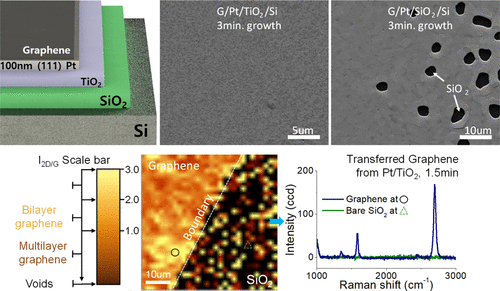
This study presents chemical vapor deposition (CVD) growth of high-quality monolayer graphene on 100 nm-thick Pt thin films deposited on TiO2-coated silicon wafers. Conventional graphene growth on Pt thin films using CVD requires relatively thick films because of potential dewetting issues, which limits fabrication integration for nano-/microelectromechanical system (NEMS/MEMS) devices. Additional metal interlayers are commonly introduced to provide good adhesion between the Pt thin film and the substrate to achieve reliable graphene growth on thinner thin films. However, growing high-quality graphene on the Pt films with a thickness of less than 100 nm has still not been demonstrated because of dewetting issues. In this work, we introduce TiO2 as an adhesion layer for Pt on a Si substrate for graphene growth and show that using this adhesion layer, we are able to achieve large-area coverage of high-quality graphene without significant surface dewetting of a 100 nm Pt thin-film substrate. These results are confirmed by time-of-flight secondary ion mass spectrometry and Raman spectroscopy measurements. Our results show that graphene growth on Pt thin films can be more reliable using TiO2 as an adhesion layer and provides a guide for integration of growth of graphene onto the NEMS/MEMS device during the fabrication process.
中文翻译:

在纳米和纳米机电系统上沉积在TiO 2基底上的纳米级Pt膜上生长的单层石墨烯
这项研究提出了高质量的单层石墨烯在沉积在TiO 2涂层的硅片上的100 nm厚的Pt薄膜上的化学气相沉积(CVD)生长。由于潜在的反润湿问题,使用CVD在Pt薄膜上进行常规石墨烯生长需要相对厚的膜,这限制了纳米/微机电系统(NEMS / MEMS)器件的制造集成度。通常引入附加的金属夹层,以在Pt薄膜和基材之间提供良好的粘合性,从而在较薄的薄膜上实现可靠的石墨烯生长。然而,由于去湿的问题,尚未证明在小于100nm的厚度的Pt膜上生长高质量的石墨烯。在这项工作中,我们介绍了TiO 2作为用于石墨烯生长的Si衬底上Pt的粘合层,并显示出使用该粘合层,我们能够实现高质量石墨烯的大面积覆盖,而不会显着润湿100 nm Pt薄膜衬底。这些结果通过飞行时间二次离子质谱和拉曼光谱测量得到证实。我们的结果表明,使用TiO 2作为粘附层,可以使Pt薄膜上的石墨烯生长更加可靠,并为在制造过程中将石墨烯的生长整合到NEMS / MEMS器件上提供了指导。
更新日期:2020-10-25
中文翻译:
在纳米和纳米机电系统上沉积在TiO 2基底上的纳米级Pt膜上生长的单层石墨烯
这项研究提出了高质量的单层石墨烯在沉积在TiO 2涂层的硅片上的100 nm厚的Pt薄膜上的化学气相沉积(CVD)生长。由于潜在的反润湿问题,使用CVD在Pt薄膜上进行常规石墨烯生长需要相对厚的膜,这限制了纳米/微机电系统(NEMS / MEMS)器件的制造集成度。通常引入附加的金属夹层,以在Pt薄膜和基材之间提供良好的粘合性,从而在较薄的薄膜上实现可靠的石墨烯生长。然而,由于去湿的问题,尚未证明在小于100nm的厚度的Pt膜上生长高质量的石墨烯。在这项工作中,我们介绍了TiO 2作为用于石墨烯生长的Si衬底上Pt的粘合层,并显示出使用该粘合层,我们能够实现高质量石墨烯的大面积覆盖,而不会显着润湿100 nm Pt薄膜衬底。这些结果通过飞行时间二次离子质谱和拉曼光谱测量得到证实。我们的结果表明,使用TiO 2作为粘附层,可以使Pt薄膜上的石墨烯生长更加可靠,并为在制造过程中将石墨烯的生长整合到NEMS / MEMS器件上提供了指导。


 京公网安备 11010802027423号