当前位置:
X-MOL 学术
›
ACS Appl. Energy Mater.
›
论文详情
Our official English website, www.x-mol.net, welcomes your
feedback! (Note: you will need to create a separate account there.)
Relating the 3D Geometry and Photoelectrochemical Activity of WO3-Loaded n-Si Nanowires: Design Rules for Photoelectrodes
ACS Applied Energy Materials ( IF 5.4 ) Pub Date : 2020-09-09 , DOI: 10.1021/acsaem.0c01115 Yihui Zhao 1 , Shashank Balasubramanyam 2 , Ageeth. A. Bol 2 , Anja Bieberle-Hütter 1
ACS Applied Energy Materials ( IF 5.4 ) Pub Date : 2020-09-09 , DOI: 10.1021/acsaem.0c01115 Yihui Zhao 1 , Shashank Balasubramanyam 2 , Ageeth. A. Bol 2 , Anja Bieberle-Hütter 1
Affiliation
|
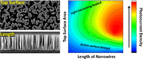
Nanostructured electrodes for photoelectrochemical (PEC) applications, such as water splitting, have a rather low photocurrent density regarding their highly enlarged surface area compared to plain electrodes. This demands for further understanding of the relation between the three-dimensional (3D) geometry and the PEC activity. To this end, we fabricate WO3/Si nanowire array photoanodes with various nanowire lengths (1.3, 2.7, 3.2, and 3.8 μm) and different WO3 thicknesses (10, 30, and 50 nm) using wet chemical etching for nanostructuring of Si and atomic layer deposition for the deposition of WO3. It is found that by increasing the etching time, the nanowires become longer and the top surface area decreases. The photocurrent density first increases and then decreases with increasing Si etching time. This behavior can be explained by different and opposite effects regarding absorption, geometry, and material-specific properties. Particularly, the decrease of the photocurrent density can be due to: (1) the longer the nanowires, the heavier the recombination of the photogenerated carriers and (2) the long-time Si etching results in a loss of top part of the nanowire arrays. Because of shadowing, the WO3 located at the top part of the nanowires is more effective than that at the bottom part for the WO3/Si nanowire arrays and therefore the photocurrent is decreased. It reveals a trade-off between the top part surface area and the length of the nanowires. This study contributes to a better understanding of the relation between the geometry of nanostructures and the performance of PEC electrodes.
中文翻译:

WO 3负载的n-Si纳米线的3D几何形状和光电化学活性的关系:光电极的设计规则
与平面电极相比,用于光化学(PEC)应用(例如水分解)的纳米结构电极具有很高的表面积,因此具有较低的光电流密度。这就要求进一步了解三维(3D)几何形状与PEC活动之间的关系。为此,我们使用湿法化学刻蚀技术制造了具有各种纳米线长度(1.3、2.7、3.2和3.8μm)和不同WO 3厚度(10、30和50 nm)的WO 3 / Si纳米线阵列光阳极。和原子层沉积,用于WO 3的沉积。已经发现,通过增加蚀刻时间,纳米线变长并且顶表面积减小。随着Si刻蚀时间的增加,光电流密度首先增加,然后减小。可以通过有关吸收,几何形状和特定于材料的特性的不同和相反的作用来解释此行为。特别地,光电流密度的降低可能归因于:(1)纳米线越长,光生载流子的复合越重;(2)长时间的Si蚀刻导致纳米线阵列顶部的损失。由于有阴影,位于纳米线顶部的WO 3比位于底部的WO 3更有效。/ Si纳米线阵列,因此光电流降低。它揭示了顶部表面积和纳米线长度之间的权衡。这项研究有助于更好地理解纳米结构的几何形状与PEC电极性能之间的关系。
更新日期:2020-10-26
中文翻译:
WO 3负载的n-Si纳米线的3D几何形状和光电化学活性的关系:光电极的设计规则
与平面电极相比,用于光化学(PEC)应用(例如水分解)的纳米结构电极具有很高的表面积,因此具有较低的光电流密度。这就要求进一步了解三维(3D)几何形状与PEC活动之间的关系。为此,我们使用湿法化学刻蚀技术制造了具有各种纳米线长度(1.3、2.7、3.2和3.8μm)和不同WO 3厚度(10、30和50 nm)的WO 3 / Si纳米线阵列光阳极。和原子层沉积,用于WO 3的沉积。已经发现,通过增加蚀刻时间,纳米线变长并且顶表面积减小。随着Si刻蚀时间的增加,光电流密度首先增加,然后减小。可以通过有关吸收,几何形状和特定于材料的特性的不同和相反的作用来解释此行为。特别地,光电流密度的降低可能归因于:(1)纳米线越长,光生载流子的复合越重;(2)长时间的Si蚀刻导致纳米线阵列顶部的损失。由于有阴影,位于纳米线顶部的WO 3比位于底部的WO 3更有效。/ Si纳米线阵列,因此光电流降低。它揭示了顶部表面积和纳米线长度之间的权衡。这项研究有助于更好地理解纳米结构的几何形状与PEC电极性能之间的关系。


 京公网安备 11010802027423号