当前位置:
X-MOL 学术
›
Adv. Eng. Mater.
›
论文详情
Our official English website, www.x-mol.net, welcomes your
feedback! (Note: you will need to create a separate account there.)
Fabrication of Cu Wiring Touch Sensor via Laser Sintering of Cu Nano/Microparticle Paste on 3D‐Printed Substrate
Advanced Engineering Materials ( IF 3.4 ) Pub Date : 2020-09-09 , DOI: 10.1002/adem.202000688 Hyeon-Sik Ahn 1, 2 , Ae-Sun Oh 1 , Dong-Hwan Kim 1, 3 , Yoonseuk Choi 2 , Kyung-Hyun Kim 1 , Hyun-Cheol Bae 1, 3
Advanced Engineering Materials ( IF 3.4 ) Pub Date : 2020-09-09 , DOI: 10.1002/adem.202000688 Hyeon-Sik Ahn 1, 2 , Ae-Sun Oh 1 , Dong-Hwan Kim 1, 3 , Yoonseuk Choi 2 , Kyung-Hyun Kim 1 , Hyun-Cheol Bae 1, 3
Affiliation
|
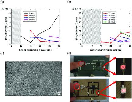
This study investigates the applications of 3D printing technology in the wiring process used in the field of electronic packaging. A Cu wiring process is developed to replace the expensive Ag‐based alternative primarily used in commercial 3D electronic circuit printing as per industry standards. The substrates needed for our experiments are developed using a 3D printer assembled prior to the research, through which poly‐ether‐ether‐ketone (PEEK) proves to be a high‐strength, high heat‐resistance material capable of undergoing the packaging process. The Cu wiring process is performed via laser sintering in ambient condition using a Cu micro/nanoparticle paste. Adopting this method minimizes the cost and duration of the process without relying on inert atmosphere generation. The optimum laser sintering condition for the Cu paste is found to be two consecutive scans at 20 W. Energy dispersive X‐ray spectroscopy (EDS) measurements show that the oxidation of the surface is about 1.35%, and further oxidation is prevented through epoxy molding. The touch sensor by Cu wiring module operate optimally even a month after its manufacture. 3D printing technology proves to be capable of replacing the wiring process used for electronic packaging.
中文翻译:

通过在3D打印的基板上激光烧结铜纳米/微粒浆料来制造铜线触摸传感器
这项研究调查了3D打印技术在电子包装领域中使用的布线过程中的应用。开发铜布线工艺以取代根据行业标准主要用于商业3D电子电路打印的昂贵的基于银的替代品。我们的实验所需的基材是使用在研究之前组装的3D打印机开发的,通过该3D打印机,聚醚醚酮(PEEK)被证明是能够经受包装过程的高强度,高耐热性材料。通过使用铜微/纳米粒子糊剂在环境条件下通过激光烧结来执行铜布线工艺。采用这种方法可以最大程度地降低过程成本和持续时间,而无需依赖于惰性气氛的产生。发现铜浆的最佳激光烧结条件是在20 W下连续扫描两次。能量色散X射线光谱(EDS)测量表明,表面氧化约为1.35%,并且通过环氧模塑可防止进一步氧化。使用Cu接线模块的触摸传感器即使在制造一个月后仍可实现最佳运行。3D打印技术被证明能够替代用于电子包装的布线工艺。
更新日期:2020-09-09
中文翻译:
通过在3D打印的基板上激光烧结铜纳米/微粒浆料来制造铜线触摸传感器
这项研究调查了3D打印技术在电子包装领域中使用的布线过程中的应用。开发铜布线工艺以取代根据行业标准主要用于商业3D电子电路打印的昂贵的基于银的替代品。我们的实验所需的基材是使用在研究之前组装的3D打印机开发的,通过该3D打印机,聚醚醚酮(PEEK)被证明是能够经受包装过程的高强度,高耐热性材料。通过使用铜微/纳米粒子糊剂在环境条件下通过激光烧结来执行铜布线工艺。采用这种方法可以最大程度地降低过程成本和持续时间,而无需依赖于惰性气氛的产生。发现铜浆的最佳激光烧结条件是在20 W下连续扫描两次。能量色散X射线光谱(EDS)测量表明,表面氧化约为1.35%,并且通过环氧模塑可防止进一步氧化。使用Cu接线模块的触摸传感器即使在制造一个月后仍可实现最佳运行。3D打印技术被证明能够替代用于电子包装的布线工艺。


 京公网安备 11010802027423号