当前位置:
X-MOL 学术
›
Plasma Processes Polym.
›
论文详情
Our official English website, www.x-mol.net, welcomes your
feedback! (Note: you will need to create a separate account there.)
Effect of temperature and incident ion energy on nanostructure formation on silicon exposed to helium plasma
Plasma Processes and Polymers ( IF 2.9 ) Pub Date : 2020-09-06 , DOI: 10.1002/ppap.202000126 Matt Thompson 1 , Quan Shi 2 , Shin Kajita 3 , Noriyasu Ohno 2 , Cormac Corr 1
Plasma Processes and Polymers ( IF 2.9 ) Pub Date : 2020-09-06 , DOI: 10.1002/ppap.202000126 Matt Thompson 1 , Quan Shi 2 , Shin Kajita 3 , Noriyasu Ohno 2 , Cormac Corr 1
Affiliation
|
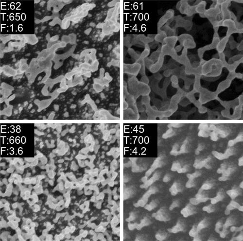
Helium plasma can be used to deliver low‐energy (<100 eV) helium ions to stimulate the growth of nanostructures on silicon surfaces. This can produce a wide range of surface features including nanoscale roughening, nanowires and porous structures. In this study, nanostructure sizes varied from ∼10 to over 100 nm in diameter. The effect of these structures on surface reflectivity for photovoltaic and photocatalytic applications is also investigated. Broadband suppression of photoreflectivity is achieved across the 300–1,200 nm wavelength range studied for silicon exposed to helium plasma at 600°C, with an average reflectivity of 3.2% and 2.9% for incident helium ion energies of 42 and 62 eV, respectively.
中文翻译:

温度和入射离子能量对暴露于氦等离子体的硅纳米结构形成的影响
氦等离子体可用于传递低能(<100 eV)氦离子,以刺激硅表面上纳米结构的生长。这可以产生广泛的表面特征,包括纳米级粗糙化,纳米线和多孔结构。在这项研究中,纳米结构的大小从10纳米到100纳米以上不等。还研究了这些结构对光伏和光催化应用的表面反射率的影响。对于在600°C下暴露于氦等离子体的硅进行了研究,在300–1,200 nm波长范围内实现了光反射率的宽带抑制,入射氦离子能量分别为42 eV和62 eV时,平均反射率分别为3.2%和2.9%。
更新日期:2020-09-06
中文翻译:
温度和入射离子能量对暴露于氦等离子体的硅纳米结构形成的影响
氦等离子体可用于传递低能(<100 eV)氦离子,以刺激硅表面上纳米结构的生长。这可以产生广泛的表面特征,包括纳米级粗糙化,纳米线和多孔结构。在这项研究中,纳米结构的大小从10纳米到100纳米以上不等。还研究了这些结构对光伏和光催化应用的表面反射率的影响。对于在600°C下暴露于氦等离子体的硅进行了研究,在300–1,200 nm波长范围内实现了光反射率的宽带抑制,入射氦离子能量分别为42 eV和62 eV时,平均反射率分别为3.2%和2.9%。


 京公网安备 11010802027423号