Nano Research ( IF 9.5 ) Pub Date : 2020-08-08 , DOI: 10.1007/s12274-020-2968-5 Thanh Luan Phan , Dinh Loc Duong , Tuan Khanh Chau , Sidi Fan , Won Tae Kang , Thi Suong Le , Hyun Yong Song , Linfeng Sun , Van Tu Vu , Min Ji Lee , Quoc An Vu , Young Hee Lee , Woo Jong Yu
|
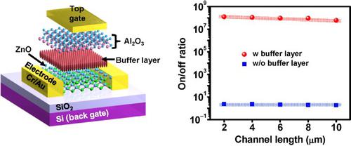
The interface between oxide/oxide layers shows an inhomogeneous charge transport behavior, which reveals a high conductivity owing to interface-doped. One typical example is the hetero-interface between ZnO film and other wide band gap oxides (e.g., Al2O3, TiO2, and HfO2). It is thus quite evident that the ZnO/other oxides hetero-interface contains high density electron carriers effectively screening the gate-induced electric field. Thus, an extremely weak gate modulation in ZnO film was showed, resulting in very low on/off ratio of 1.69 in top-gate field-effect-transistor (TG-FET) configuration. So, to extend the usage of ZnO TG-FET is not quite possible toward further practical application. Herein, we clarified the correlation of inhomogeneous region in oxide/oxide hetero-junction by systematically study. Our work suggests that a self-assembly of molecules (SAM) buffer layer is suitable for tuning the inhomogeneous charge transport in ZnO film, which not only reduces the interface trap density, but also effectively enhances the gate electric field modulation at the hetero-interface. We further report the robust fabrication of TG-FET arrays based on ZnO thin film, using an ultra-thin alkylphosphonic acid molecule monolayer as buffer layer. Our device demonstrates a pronounced ultrahigh on/off ratio of ≥ 108, which is 8-order of magnitude higher than that of a device without buffer layer. For the highly reliable arrays, our device exhibits a high yield of over 93% with an average on/off ratio of ~107 across the entire wafer scale, mobility (18.5 cm2/(V·s)), an extended bias-stressing (~ 2,000 s) and long-stability (~ 150 days) under ambient conditions.
中文翻译:
调整ZnO接口中的不均匀电荷传输,以实现超高通/断比的顶栅场效应晶体管阵列
氧化物/氧化物层之间的界面显示出不均匀的电荷传输行为,这归因于界面掺杂而显示出高电导率。一个典型的例子是ZnO薄膜和其他宽带隙氧化物(例如Al 2 O 3,TiO 2和HfO 2)之间的异质界面)。因此,很明显,ZnO /其他氧化物的异质界面包含高密度电子载流子,可有效地屏蔽栅极感应电场。因此,显示出ZnO膜中极弱的栅极调制,导致顶栅场效应晶体管(TG-FET)配置中的导通/截止比非常低,为1.69。因此,扩展ZnO TG-FET的用途不太可能进一步走向实际应用。在本文中,我们通过系统研究阐明了氧化物/氧化物异质结中不均匀区域的相关性。我们的工作表明分子自组装(SAM)缓冲层适用于调节ZnO膜中的不均匀电荷传输,这不仅降低了界面陷阱密度,而且有效地增强了异质界面上的栅极电场调制。我们进一步报告了使用超薄烷基膦酸分子单层作为缓冲层,基于ZnO薄膜的TG-FET阵列的稳健制造。我们的设备显示出显着的超高开/关比,≥10与图8相比,它比没有缓冲层的器件高8个数量级。对于高度可靠的阵列,我们的设备在整个晶圆尺寸,迁移率(18.5 cm 2 /(V·s)),扩展的偏置电压下具有93%以上的高产率,平均开/关比约为10 7在环境条件下承受压力(〜2,000 s)和长期稳定性(〜150天)。


 京公网安备 11010802027423号