当前位置:
X-MOL 学术
›
ACS Appl. Mater. Interfaces
›
论文详情
Our official English website, www.x-mol.net, welcomes your
feedback! (Note: you will need to create a separate account there.)
The Role of Metal-Semiconductor Interface in Halide Perovskite Devices for Radiation Photon Counting.
ACS Applied Materials & Interfaces ( IF 8.3 ) Pub Date : 2020-09-04 , DOI: 10.1021/acsami.0c11805 Shreetu Shrestha 1 , Hsinhan Tsai 1 , Michael Yoho 2 , Dibyajyoti Ghosh 3 , Fangze Liu 1 , Yusheng Lei 4 , Jeremy Tisdale 1 , Jon Baldwin 1, 5 , Sheng Xu 4 , Amanda J Neukirch 3 , Sergei Tretiak 3 , Duc Vo 2 , Wanyi Nie 1, 5
ACS Applied Materials & Interfaces ( IF 8.3 ) Pub Date : 2020-09-04 , DOI: 10.1021/acsami.0c11805 Shreetu Shrestha 1 , Hsinhan Tsai 1 , Michael Yoho 2 , Dibyajyoti Ghosh 3 , Fangze Liu 1 , Yusheng Lei 4 , Jeremy Tisdale 1 , Jon Baldwin 1, 5 , Sheng Xu 4 , Amanda J Neukirch 3 , Sergei Tretiak 3 , Duc Vo 2 , Wanyi Nie 1, 5
Affiliation
|
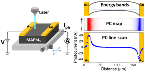
Halide perovskites are promising optoelectronic semiconductors. For applications in solid-state detectors that operate in low photon flux counting mode, blocking interfaces are essential to minimize the dark current noise. Here, we investigate the interface between methylammonium lead tri-iodide (MAPbI3) single crystals and commonly used high and low work function metals to achieve photon counting capabilities in a solid-state detector. Using scanning photocurrent microscopy, we observe a large Schottky barrier at the MAPbI3/Pb interface, which efficiently blocks dark current. Moreover, the shape of the photocurrent profile indicates that the MAPbI3 single-crystal surface has a deep fermi level close to that of Au. Rationalized by first-principle calculations, we attribute this observation to the defects due to excess iodine on the surface underpinning emergence of deep band-edge states. The photocurrent decay profile yields a charge carrier diffusion length of 10–25 μm. Using this knowledge, we demonstrate a single-crystal MAPbI3 detector that can count single γ-ray photons by producing sharp electrical pulses with a fast rise time of <2 μs. Our study indicates that the interface plays a crucial role in solid-state detectors operating in photon counting mode.
中文翻译:

金属半导体界面在辐射光子计数的卤化物钙钛矿设备中的作用。
卤化物钙钛矿是有前途的光电半导体。对于在低光子通量计数模式下工作的固态检测器中的应用,阻塞接口对于最大程度地减小暗电流噪声至关重要。在这里,我们研究了甲基铵三碘化铅(MAPbI 3)单晶与常用的高和低功函数金属之间的界面,以在固态检测器中实现光子计数功能。使用扫描光电流显微镜,我们在MAPbI 3 / Pb界面观察到一个大的肖特基势垒,该势垒有效地阻止了暗电流。此外,光电流轮廓的形状表明MAPbI 3单晶表面的深费米能级接近Au。通过第一性原理计算的合理化,我们将此观察结果归因于表面上过量碘导致的缺陷,这些缺陷支撑了深能带状态的出现。光电流衰减曲线产生的电荷载流子扩散长度为10–25μm。利用这一知识,我们展示了单晶MAPbI 3检测器,该检测器可以通过产生尖锐的电脉冲并以小于2μs的快速上升时间来计数单个γ射线光子。我们的研究表明,该接口在以光子计数模式运行的固态检测器中起着至关重要的作用。
更新日期:2020-10-07
中文翻译:
金属半导体界面在辐射光子计数的卤化物钙钛矿设备中的作用。
卤化物钙钛矿是有前途的光电半导体。对于在低光子通量计数模式下工作的固态检测器中的应用,阻塞接口对于最大程度地减小暗电流噪声至关重要。在这里,我们研究了甲基铵三碘化铅(MAPbI 3)单晶与常用的高和低功函数金属之间的界面,以在固态检测器中实现光子计数功能。使用扫描光电流显微镜,我们在MAPbI 3 / Pb界面观察到一个大的肖特基势垒,该势垒有效地阻止了暗电流。此外,光电流轮廓的形状表明MAPbI 3单晶表面的深费米能级接近Au。通过第一性原理计算的合理化,我们将此观察结果归因于表面上过量碘导致的缺陷,这些缺陷支撑了深能带状态的出现。光电流衰减曲线产生的电荷载流子扩散长度为10–25μm。利用这一知识,我们展示了单晶MAPbI 3检测器,该检测器可以通过产生尖锐的电脉冲并以小于2μs的快速上升时间来计数单个γ射线光子。我们的研究表明,该接口在以光子计数模式运行的固态检测器中起着至关重要的作用。


 京公网安备 11010802027423号