当前位置:
X-MOL 学术
›
Mater. Today Phys.
›
论文详情
Our official English website, www.x-mol.net, welcomes your
feedback! (Note: you will need to create a separate account there.)
Ultra-High Critical Electric Field of 13.2 MV/cm for Zn-doped p-type β-Ga2O3
Materials Today Physics ( IF 10.0 ) Pub Date : 2020-12-01 , DOI: 10.1016/j.mtphys.2020.100263 E. Chikoidze , T. Tchelidze , C. Sartel , Z. Chi , R. Kabouche , I. Madaci , C. Rubio , H. Mohamed , V. Sallet , F. Medjdoub , A. Perez-Tomas , Y. Dumont
Materials Today Physics ( IF 10.0 ) Pub Date : 2020-12-01 , DOI: 10.1016/j.mtphys.2020.100263 E. Chikoidze , T. Tchelidze , C. Sartel , Z. Chi , R. Kabouche , I. Madaci , C. Rubio , H. Mohamed , V. Sallet , F. Medjdoub , A. Perez-Tomas , Y. Dumont
|
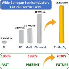
Abstract Which the actual critical electrical field of the ultra-wide bandgap semiconductor β-Ga2O3 is? Even that it is usual to find in the literature a given value for the critical field of wide and ultra-wide semiconductors such as SiC (3 MV/cm), GaN (3.3 MV/cm), β-Ga2O3 (~8 MV/cm) and diamond (10 MV/cm), this value actually depends on intrinsic and extrinsic factors such as the bandgap energy, material residual impurities or introduced dopants. Indeed, it is well known from 1950's that reducing the residual doping (NB) of the semiconductor layer increases the breakdown voltage capability of a semiconductor media (e.g. as N B − 3 / 4 by using the Fulop's approximation for an abrupt junction). A key limitation is, therefore, the residual donor/acceptor concentration generally found in these materials. Here, we report that doping with amphoteric Zinc a p-type β-Ga2O3 thin films shortens free carrier mean free path (0.37 nm), resulting in the ultra-high critical electrical field of 13.2 MV/cm. Therefore, the critical breakdown field can be, at least, four times larger for the emerging Ga2O3 power semiconductor as compared to SiC and GaN. We further explain these wide-reaching experimental facts by using theoretical approaches based on the impact ionization microscopic theory and thermodynamic calculations.
中文翻译:

Zn掺杂p型β-Ga2O3的13.2 MV/cm超高临界电场
摘要 超宽带隙半导体β-Ga2O3的实际临界电场是哪一个?即使通常在文献中找到宽和超宽半导体的临界场的给定值,例如 SiC (3 MV/cm)、GaN (3.3 MV/cm)、β-Ga2O3 (~8 MV/cm) cm) 和金刚石 (10 MV/cm),该值实际上取决于内在和外在因素,例如带隙能量、材料残留杂质或引入的掺杂剂。事实上,从 1950 年代开始就众所周知,减少半导体层的残留掺杂 (NB) 会增加半导体介质的击穿电压能力(例如,通过使用 Fulop 近似来计算突变结,可以提高 NB - 3 / 4)。因此,一个关键的限制是,通常在这些材料中发现的残留供体/受体浓度。这里,我们报告说,掺杂两性锌 a p 型 β-Ga2O3 薄膜可缩短自由载流子平均自由程(0.37 nm),从而产生 13.2 MV/cm 的超高临界电场。因此,与 SiC 和 GaN 相比,新兴的 Ga2O3 功率半导体的临界击穿场至少可以大四倍。我们通过使用基于碰撞电离微观理论和热力学计算的理论方法进一步解释了这些影响广泛的实验事实。
更新日期:2020-12-01
中文翻译:
Zn掺杂p型β-Ga2O3的13.2 MV/cm超高临界电场
摘要 超宽带隙半导体β-Ga2O3的实际临界电场是哪一个?即使通常在文献中找到宽和超宽半导体的临界场的给定值,例如 SiC (3 MV/cm)、GaN (3.3 MV/cm)、β-Ga2O3 (~8 MV/cm) cm) 和金刚石 (10 MV/cm),该值实际上取决于内在和外在因素,例如带隙能量、材料残留杂质或引入的掺杂剂。事实上,从 1950 年代开始就众所周知,减少半导体层的残留掺杂 (NB) 会增加半导体介质的击穿电压能力(例如,通过使用 Fulop 近似来计算突变结,可以提高 NB - 3 / 4)。因此,一个关键的限制是,通常在这些材料中发现的残留供体/受体浓度。这里,我们报告说,掺杂两性锌 a p 型 β-Ga2O3 薄膜可缩短自由载流子平均自由程(0.37 nm),从而产生 13.2 MV/cm 的超高临界电场。因此,与 SiC 和 GaN 相比,新兴的 Ga2O3 功率半导体的临界击穿场至少可以大四倍。我们通过使用基于碰撞电离微观理论和热力学计算的理论方法进一步解释了这些影响广泛的实验事实。


 京公网安备 11010802027423号