当前位置:
X-MOL 学术
›
J. Soc. Inf. Disp.
›
论文详情
Our official English website, www.x-mol.net, welcomes your
feedback! (Note: you will need to create a separate account there.)
Organic light‐emitting diode display pixel circuit employing double‐gate low‐temperature poly‐Si thin‐film transistor and metal‐oxide thin‐film transistors
Journal of the Society for Information Display ( IF 1.7 ) Pub Date : 2020-09-01 , DOI: 10.1002/jsid.961 JoonHo Lee 1 , DaeHyun Kim 1 , JooWon Yang 1 , KookChul Moon 1 , Soo‐Yeon Lee 2 , JaeHong Jeon 3 , YongSang Kim 4 , SeungChan Choi 5 , UiJin Chung 5 , KwonShik Park 5 , KeeChan Park 1
Journal of the Society for Information Display ( IF 1.7 ) Pub Date : 2020-09-01 , DOI: 10.1002/jsid.961 JoonHo Lee 1 , DaeHyun Kim 1 , JooWon Yang 1 , KookChul Moon 1 , Soo‐Yeon Lee 2 , JaeHong Jeon 3 , YongSang Kim 4 , SeungChan Choi 5 , UiJin Chung 5 , KwonShik Park 5 , KeeChan Park 1
Affiliation
|
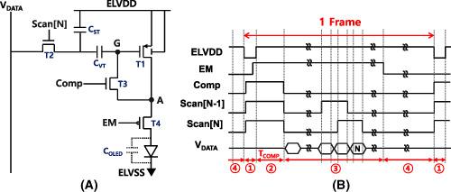
An organic light‐emitting diode (OLED) display pixel circuit composed of a double‐gate (DG) low‐temperature polycrystalline silicon (LTPS) thin‐film transistor (TFT) and metal‐oxide (MO) TFTs is reported. Two control lines used to initialize the gate‐to‐source bias (VGS) of the driving TFT in the conventional pixel circuit are eliminated by modulating the bottom gate bias (VBS) of the DG‐LTPS TFT. Low leakage current of MO TFT enables us to adopt the simultaneous‐emission scheme for arbitrary compensation time setting and 1‐Hz frame rate driving for low power consumption without flicker. The proposed circuit exhibits better compensation results and smaller area compared with the conventional low‐temperature polycrystalline silicon and oxide (LTPO) pixel circuit. The pixel density of 538 pixels per inch (ppi) has been obtained employing 2‐μm design rule.
中文翻译:

采用双栅极低温多晶硅薄膜晶体管和金属氧化物薄膜晶体管的有机发光二极管显示像素电路
据报道,有机发光二极管(OLED)显示像素电路由双栅极(DG)低温多晶硅(LTPS)薄膜晶体管(TFT)和金属氧化物(MO)TFT组成。通过调制底部栅极偏置(V BS),消除了用于初始化常规像素电路中驱动TFT的栅极至源极偏置(V GS)的两条控制线)。MO TFT的低泄漏电流使我们能够采用同时发射方案进行任意补偿时间设置,并采用1-Hz帧频驱动,以实现低功耗而无闪烁。与传统的低温多晶硅和氧化物(LTPO)像素电路相比,该电路具有更好的补偿效果和更小的面积。采用2μm设计规则获得了538像素/英寸(ppi)的像素密度。
更新日期:2020-09-01
中文翻译:
采用双栅极低温多晶硅薄膜晶体管和金属氧化物薄膜晶体管的有机发光二极管显示像素电路
据报道,有机发光二极管(OLED)显示像素电路由双栅极(DG)低温多晶硅(LTPS)薄膜晶体管(TFT)和金属氧化物(MO)TFT组成。通过调制底部栅极偏置(V BS),消除了用于初始化常规像素电路中驱动TFT的栅极至源极偏置(V GS)的两条控制线)。MO TFT的低泄漏电流使我们能够采用同时发射方案进行任意补偿时间设置,并采用1-Hz帧频驱动,以实现低功耗而无闪烁。与传统的低温多晶硅和氧化物(LTPO)像素电路相比,该电路具有更好的补偿效果和更小的面积。采用2μm设计规则获得了538像素/英寸(ppi)的像素密度。


 京公网安备 11010802027423号