Our official English website, www.x-mol.net, welcomes your
feedback! (Note: you will need to create a separate account there.)
Encapsulation of Nanostructures in a Dielectric Matrix Providing Optical Enhancement in Ultrathin Solar Cells
Solar RRL ( IF 6.0 ) Pub Date : 2020-08-29 , DOI: 10.1002/solr.202000310 António J. N. Oliveira 1 , Jessica de Wild 2, 3, 4 , Kevin Oliveira 1 , Beatriz A. Valença 1 , Jennifer P. Teixeira 1 , Joana R. L. Guerreiro 1 , Sara Abalde-Cela 1 , Tomás S. Lopes 1, 2, 3, 4 , Rodrigo M. Ribeiro 1, 5 , José M. V. Cunha 1, 6, 7 , Marco A. Curado 1, 8 , Margarida Monteiro 1, 9 , André Violas 1, 5 , Ana Gomes Silva 9, 10 , Marta Prado 1 , Paulo A. Fernandes 1, 6, 11 , Bart Vermang 2, 3, 4 , Pedro M. P. Salomé 1, 7
Solar RRL ( IF 6.0 ) Pub Date : 2020-08-29 , DOI: 10.1002/solr.202000310 António J. N. Oliveira 1 , Jessica de Wild 2, 3, 4 , Kevin Oliveira 1 , Beatriz A. Valença 1 , Jennifer P. Teixeira 1 , Joana R. L. Guerreiro 1 , Sara Abalde-Cela 1 , Tomás S. Lopes 1, 2, 3, 4 , Rodrigo M. Ribeiro 1, 5 , José M. V. Cunha 1, 6, 7 , Marco A. Curado 1, 8 , Margarida Monteiro 1, 9 , André Violas 1, 5 , Ana Gomes Silva 9, 10 , Marta Prado 1 , Paulo A. Fernandes 1, 6, 11 , Bart Vermang 2, 3, 4 , Pedro M. P. Salomé 1, 7
Affiliation
|
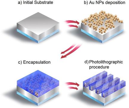
The incorporation of nanostructures in optoelectronic devices for enhancing their optical performance is widely studied. However, several problems related to the processing complexity and the low performance of the nanostructures have hindered such actions in real‐life devices. Herein, a novel way of introducing gold nanoparticles in a solar cell structure is proposed in which the nanostructures are encapsulated with a dielectric layer, shielding them from high temperatures and harsh growth processing conditions of the remaining device. Through optical simulations, an enhancement of the effective optical path length of approximately four times the nominal thickness of the absorber layer is verified with the new architecture. Furthermore, the proposed concept in a Cu(In,Ga)Se2 solar cell device is demonstrated, where the short‐circuit current density is increased by 17.4%. The novel structure presented in this work is achieved by combining a bottom‐up chemical approach of depositing the nanostructures with a top‐down photolithographic process, which allows for an electrical contact.
中文翻译:

在超薄太阳能电池中提供光学增强的介电基质中纳米结构的封装
广泛研究了将纳米结构引入光电器件中以增强其光学性能。但是,与加工复杂性和纳米结构的低性能有关的一些问题阻碍了现实生活中的设备中的此类行为。在此,提出了一种在太阳能电池结构中引入金纳米颗粒的新颖方法,其中该纳米结构被介电层封装,使它们免受高温和其余器件的苛刻生长工艺条件的影响。通过光学仿真,新架构证实了有效光路长度的增加约为吸收层标称厚度的四倍。此外,在Cu(In,Ga)Se 2中提出的概念演示了太阳能电池装置,其中短路电流密度增加了17.4%。通过结合自下而上的化学沉积纳米结构的方法和自上而下的光刻工艺(可实现电接触),可以实现这项工作中提出的新颖结构。
更新日期:2020-11-06
中文翻译:
在超薄太阳能电池中提供光学增强的介电基质中纳米结构的封装
广泛研究了将纳米结构引入光电器件中以增强其光学性能。但是,与加工复杂性和纳米结构的低性能有关的一些问题阻碍了现实生活中的设备中的此类行为。在此,提出了一种在太阳能电池结构中引入金纳米颗粒的新颖方法,其中该纳米结构被介电层封装,使它们免受高温和其余器件的苛刻生长工艺条件的影响。通过光学仿真,新架构证实了有效光路长度的增加约为吸收层标称厚度的四倍。此外,在Cu(In,Ga)Se 2中提出的概念演示了太阳能电池装置,其中短路电流密度增加了17.4%。通过结合自下而上的化学沉积纳米结构的方法和自上而下的光刻工艺(可实现电接触),可以实现这项工作中提出的新颖结构。


 京公网安备 11010802027423号