Sensors and Actuators A: Physical ( IF 4.1 ) Pub Date : 2020-08-27 , DOI: 10.1016/j.sna.2020.112309 A. Garzon-Roman , D.H. Cuate-Gomez , C. Zuñiga-Islas , J.L. Sosa-Sanchez , F. Lopez-Huerta
|
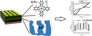
Organic semiconductors have recently gained more attention due to their electrical properties and flexibility for combining with other materials, mainly with inorganic semiconductors (silicon). In this work we fabricated heterostructures based on Erbium phthalocyanine (ErPc) on porous silicon (PS) and crystalline silicon (c-Si). The ErPc was synthetized by a solar reaction procedure and deposited on PS and c-Si substrates by sublimation. The PS was obtained by using Metal-Assisted Chemical Etching. We characterized the morphological, optical, and electrical properties of these heterostructures to study their behavior and to propose an optoelectronic application for them. The morphology of the ErPc film resulted in structural differences depending on the substrate; for the case of the silicon substrate, we only found micro-rod structures uniformly distributed and, on porous silicon layers, we obtained a combination of nanoparticles and nanotubes according to the FE-SEM characterization. The diffuse reflectance spectrum of the erbium phthalocyanine showed the lowest reflectance, which is an important parameter for optoelectronic applications to reduce loses from reflectivity. The absorbance spectrum showed the three main bands that identified the presence of the ErPc complex. The heterostructures displayed a rectifying and ohmic behavior in the I–V curves. In addition, a photocurrent effect was observed, but only at high voltages. Finally, the current-time curves obtained from the heterojunctions demonstrated a clear response to white light pulses with 1 V reverse bias. The combination of organic and inorganic semiconductors can open new opportunities for application in optoelectronics.
中文翻译:
多孔硅上的酞菁:形态,光学和电学表征,可能用作光电探测器
由于有机半导体的电性能和与其他材料(主要是与无机半导体(硅)结合)的灵活性,有机半导体最近已引起更多关注。在这项工作中,我们在多孔硅(PS)和晶体硅(c-Si)上制造了基于Er酞菁(ErPc)的异质结构。通过太阳反应程序合成ErPc,并通过升华将其沉积在PS和c-Si衬底上。通过使用金属辅助化学蚀刻获得PS。我们表征了这些异质结构的形态,光学和电学性质,以研究其行为并为它们提出光电应用。ErPc膜的形态导致结构差异,具体取决于基材。对于硅基板,我们仅发现微棒结构均匀分布,并且在多孔硅层上,根据FE-SEM表征获得了纳米颗粒和纳米管的组合。酞菁的漫反射光谱显示出最低的反射率,这是光电应用中减少反射率损失的重要参数。吸收光谱显示了识别ErPc复合物存在的三个主要谱带。异质结构在IV曲线中显示出整流和欧姆行为。另外,观察到光电流效应,但仅在高电压下。最后,从异质结获得的电流时间曲线显示出对具有1 V反向偏置的白光脉冲的清晰响应。


 京公网安备 11010802027423号