当前位置:
X-MOL 学术
›
J. Mater. Res.
›
论文详情
Our official English website, www.x-mol.net, welcomes your
feedback! (Note: you will need to create a separate account there.)
A novel terbium doping effect on physical properties of lead sulfide nanostructures: A facile synthesis and characterization
Journal of Materials Research ( IF 2.7 ) Pub Date : 2020-08-26 , DOI: 10.1557/jmr.2020.216 Mohd. Shkir , Kamlesh V. Chandekar , Thamraa Alshahrani , Ashwani Kumar , Salem AlFaify
Journal of Materials Research ( IF 2.7 ) Pub Date : 2020-08-26 , DOI: 10.1557/jmr.2020.216 Mohd. Shkir , Kamlesh V. Chandekar , Thamraa Alshahrani , Ashwani Kumar , Salem AlFaify
|
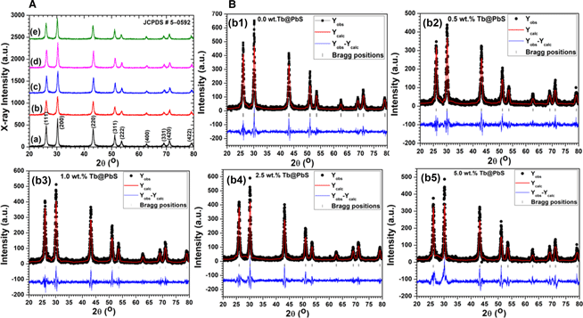
Lead sulfide (PbS) is having tremendous applications in the field of optoelectronics. Hence, a facile low temperature synthesis of PbS with different contents of terbium (Tb) has been achieved and investigated for structure–optic–dielectric–electrical properties. The structure confirmation was observed through the X-ray diffraction and Rietveld refinement process which approved a monophasic cubic structure. Rietveld refinement gives a best-fitting profile of the prepared products. The crystallite size was estimated to be in range of 15–21 nm. FT-Raman study also approved the single-phase PbS with all characteristic modes. For further confirmation of composition, homogeneity, and Tb in the final product, the EDX/SEM e-mapping was carried out. The morphological investigation was carried out through SEM which revealed that the shape and size are greatly influenced by Tb content addition in PbS. The energy gap (Eg) was estimated in the range of 1.42–1.62 eV for all Tb@PbS, and the largest Eg value was observed for 0.5 wt% Tb@PbS. The dielectric constant values are calculated in the range of 16–25 in the tested frequency region. The ac electrical conductivity was enhanced with frequency, and a charge transport mechanism is related to a correlated barrier hoping model in the prepared samples.
中文翻译:

一种新型铽掺杂对硫化铅纳米结构物理性质的影响:一种简便的合成和表征
硫化铅 (PbS) 在光电领域有着巨大的应用。因此,已经实现了具有不同铽 (Tb) 含量的 PbS 的简便低温合成,并对其结构-光学-介电-电学特性进行了研究。通过 X 射线衍射和 Rietveld 精修过程观察到结构确认,该过程证实了单相立方结构。Rietveld 细化给出了所制备产品的最佳拟合轮廓。微晶尺寸估计在 15-21 nm 的范围内。FT-Raman 研究还批准了具有所有特征模式的单相 PbS。为了进一步确认最终产品中的成分、均匀性和 Tb,进行了 EDX/SEM 电子映射。通过 SEM 进行形态学研究,结果表明形状和尺寸受 PbS 中 Tb 含量的影响很大。所有 Tb@PbS 的能隙 (Eg) 估计在 1.42-1.62 eV 的范围内,并且在 0.5 wt% Tb@PbS 时观察到最大的 Eg 值。介电常数值在测试频率区域的 16-25 范围内计算。交流电导率随着频率的增加而增强,电荷传输机制与制备的样品中的相关势垒希望模型有关。
更新日期:2020-08-26
中文翻译:
一种新型铽掺杂对硫化铅纳米结构物理性质的影响:一种简便的合成和表征
硫化铅 (PbS) 在光电领域有着巨大的应用。因此,已经实现了具有不同铽 (Tb) 含量的 PbS 的简便低温合成,并对其结构-光学-介电-电学特性进行了研究。通过 X 射线衍射和 Rietveld 精修过程观察到结构确认,该过程证实了单相立方结构。Rietveld 细化给出了所制备产品的最佳拟合轮廓。微晶尺寸估计在 15-21 nm 的范围内。FT-Raman 研究还批准了具有所有特征模式的单相 PbS。为了进一步确认最终产品中的成分、均匀性和 Tb,进行了 EDX/SEM 电子映射。通过 SEM 进行形态学研究,结果表明形状和尺寸受 PbS 中 Tb 含量的影响很大。所有 Tb@PbS 的能隙 (Eg) 估计在 1.42-1.62 eV 的范围内,并且在 0.5 wt% Tb@PbS 时观察到最大的 Eg 值。介电常数值在测试频率区域的 16-25 范围内计算。交流电导率随着频率的增加而增强,电荷传输机制与制备的样品中的相关势垒希望模型有关。


 京公网安备 11010802027423号