当前位置:
X-MOL 学术
›
Prog. Photovoltaics
›
论文详情
Our official English website, www.x-mol.net, welcomes your
feedback! (Note: you will need to create a separate account there.)
High‐quality amorphous silicon thin films for tunnel oxide passivating contacts deposited at over 150 nm/min
Progress in Photovoltaics ( IF 8.0 ) Pub Date : 2020-08-26 , DOI: 10.1002/pip.3333 Shenghao Li 1, 2 , Manuel Pomaska 1 , Jan Hoß 3 , Jan Lossen 3 , Kaifu Qiu 1, 2 , Ruijiang Hong 2 , Friedhelm Finger 1 , Uwe Rau 1 , Kaining Ding 1
Progress in Photovoltaics ( IF 8.0 ) Pub Date : 2020-08-26 , DOI: 10.1002/pip.3333 Shenghao Li 1, 2 , Manuel Pomaska 1 , Jan Hoß 3 , Jan Lossen 3 , Kaifu Qiu 1, 2 , Ruijiang Hong 2 , Friedhelm Finger 1 , Uwe Rau 1 , Kaining Ding 1
Affiliation
|
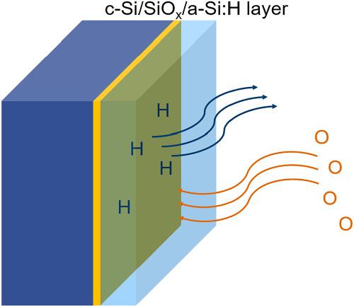
Hot‐wire chemical vapor deposition was utilized to develop rapidly grown and high‐quality phosphorus‐doped amorphous silicon (a‐Si:H) thin films for poly‐crystalline silicon on tunnel oxide carrier‐selective passivating contacts. Deposition rates higher than 150 nm/min were obtained for the in situ phosphorus‐doped a‐Si:H layers. To optimize the passivating contact performance, material properties such as microstructures as well as hydrogen content were characterized and analyzed for these phosphorus‐doped a‐Si:H films. The results show that a certain microstructure of the films is crucial for the passivation quality and the conductance of passivating contacts. Porous silicon layers were severely oxidized during high‐temperature crystallization, giving rise to very low conductance. The insufficient effective doping concentration in these layers also yields inferior passivation quality due to lack of field‐effect passivation. On the other hand, dense silicon layers are insensitive to oxidation but very sensitive to blistering of the films during the subsequent high‐temperature process steps. By optimizing the deposition parameters, a firing‐stable‐implied open‐circuit voltage of 737 mV and a contact resistivity of 10 mΩ·cm2 were achieved at a high deposition rate of 100 nm/min while 733 mV and 90 mΩ·cm2 were achieved at an even higher deposition rate of 150 nm/min.
中文翻译:

用于隧道氧化物钝化接触的高质量非晶硅薄膜,沉积速度超过150 nm / min
利用热线化学气相沉积技术,可以在隧道氧化物载流子选择性钝化触点上开发出快速生长且高质量的磷掺杂非晶硅(a-Si:H)薄膜,用于多晶硅。原位掺杂磷的a-Si:H层的沉积速率高于150 nm / min。为了优化钝化接触性能,对这些掺磷a-Si:H薄膜的材料性能(如微观结构和氢含量)进行了表征和分析。结果表明,薄膜的一定微观结构对于钝化质量和钝化接触的电导率至关重要。在高温结晶过程中,多孔硅层会被严重氧化,从而导致电导率非常低。由于缺乏场效应钝化,这些层中有效掺杂浓度不足也会导致钝化质量降低。另一方面,致密的硅层在随后的高温工艺步骤中对氧化不敏感,但对薄膜的起泡非常敏感。通过优化沉积参数,点火稳定产生的开路电压为737 mV,接触电阻率为10mΩ·cm2在100 nm / min的高沉积速率下获得,而733 mV和90mΩ·cm 2在150 nm / min的更高沉积速率下获得。
更新日期:2020-08-26
中文翻译:
用于隧道氧化物钝化接触的高质量非晶硅薄膜,沉积速度超过150 nm / min
利用热线化学气相沉积技术,可以在隧道氧化物载流子选择性钝化触点上开发出快速生长且高质量的磷掺杂非晶硅(a-Si:H)薄膜,用于多晶硅。原位掺杂磷的a-Si:H层的沉积速率高于150 nm / min。为了优化钝化接触性能,对这些掺磷a-Si:H薄膜的材料性能(如微观结构和氢含量)进行了表征和分析。结果表明,薄膜的一定微观结构对于钝化质量和钝化接触的电导率至关重要。在高温结晶过程中,多孔硅层会被严重氧化,从而导致电导率非常低。由于缺乏场效应钝化,这些层中有效掺杂浓度不足也会导致钝化质量降低。另一方面,致密的硅层在随后的高温工艺步骤中对氧化不敏感,但对薄膜的起泡非常敏感。通过优化沉积参数,点火稳定产生的开路电压为737 mV,接触电阻率为10mΩ·cm2在100 nm / min的高沉积速率下获得,而733 mV和90mΩ·cm 2在150 nm / min的更高沉积速率下获得。


 京公网安备 11010802027423号