当前位置:
X-MOL 学术
›
ACS Appl. Electron. Mater.
›
论文详情
Our official English website, www.x-mol.net, welcomes your
feedback! (Note: you will need to create a separate account there.)
Enhancing the Performance of Solution-Processed Thin-Film Transistors via Laser Scanning Annealing
ACS Applied Electronic Materials ( IF 4.3 ) Pub Date : 2020-08-24 , DOI: 10.1021/acsaelm.0c00588 Meng Xu 1 , Cong Peng 1 , Yanyu Yuan 1 , Xifeng Li 1 , Jianhua Zhang 1
ACS Applied Electronic Materials ( IF 4.3 ) Pub Date : 2020-08-24 , DOI: 10.1021/acsaelm.0c00588 Meng Xu 1 , Cong Peng 1 , Yanyu Yuan 1 , Xifeng Li 1 , Jianhua Zhang 1
Affiliation
|
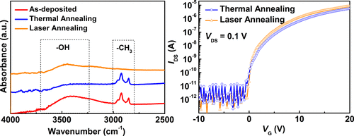
In this article, laser scanning annealing is used for the fabrication of solution-processed tungsten–zinc–tin-oxide thin-film transistors (WZTO TFTs) with low temperatures and fast processing. The high-transient intensity of the scanning laser is beneficial to the effective conversion of precursors to metal–oxide lattices, which is also verified by the X-ray photoelectron spectroscopy analysis. Moreover, no apparent phase transformation and lattice expansion exist during laser irradiation of stable amorphous structures of a-WZTO thin films, as observed from the results of X-ray diffraction, Raman scattering spectroscopy, and transmission electron microscopy. Based on laser scanning techniques, the large optical band gap (3.88 eV) is an important factor to realize a high optical performance of WZTO TFTs. The solution-processed WZTO TFT with laser scanning annealing exhibits much better performance with high mobility (up to 4.99 cm2 V–1 s–1), compared to that with thermal annealing (1.27 cm2 V–1 s–1). More importantly, this method is applicable for a wide range of metal–oxide semiconductors and polymer substrates, by solving the incompatibility between solution-processed metal–oxide semiconductors and polymer substrates because of high processing temperatures. Therefore, it shows tremendous potential to be applicable for a wide range of sensors, displays, and circuits. These results demonstrated that the laser scanning annealing provides a promising tool to simplify the fabrication of low-temperature polycrystalline oxide TFTs, when simultaneously utilizing the metal–oxide–semiconductor TFT and low-temperature polycrystalline silicon TFT processes with low cost and high yield.
中文翻译:

通过激光扫描退火提高溶液处理的薄膜晶体管的性能
在本文中,使用激光扫描退火技术以低温和快速加工的方式制造溶液加工的钨锌锌氧化物薄膜晶体管(WZTO TFT)。扫描激光的高瞬态强度有利于将前体有效转化为金属氧化物晶格,这也已通过X射线光电子能谱分析得到了验证。此外,从X射线衍射,拉曼散射光谱和透射电子显微镜的结果可以看出,在a-WZTO薄膜的稳定非晶结构的激光辐照过程中,没有明显的相变和晶格膨胀。基于激光扫描技术,大的光学带隙(3.88 eV)是实现WZTO TFT的高光学性能的重要因素。2 V –1 s –1),而热退火(1.27 cm 2 V –1 s –1))。更重要的是,该方法通过解决由于高处理温度而导致溶液处理的金属氧化物半导体与聚合物衬底之间不兼容的问题,因此适用于各种金属氧化物半导体和聚合物衬底。因此,它显示出巨大的潜力,可应用于各种传感器,显示器和电路。这些结果表明,在同时使用低成本,高产量的金属氧化物半导体TFT和低温多晶硅TFT工艺的同时,激光扫描退火为简化低温多晶硅氧化物TFT的制造提供了一种有前途的工具。
更新日期:2020-09-22
中文翻译:
通过激光扫描退火提高溶液处理的薄膜晶体管的性能
在本文中,使用激光扫描退火技术以低温和快速加工的方式制造溶液加工的钨锌锌氧化物薄膜晶体管(WZTO TFT)。扫描激光的高瞬态强度有利于将前体有效转化为金属氧化物晶格,这也已通过X射线光电子能谱分析得到了验证。此外,从X射线衍射,拉曼散射光谱和透射电子显微镜的结果可以看出,在a-WZTO薄膜的稳定非晶结构的激光辐照过程中,没有明显的相变和晶格膨胀。基于激光扫描技术,大的光学带隙(3.88 eV)是实现WZTO TFT的高光学性能的重要因素。2 V –1 s –1),而热退火(1.27 cm 2 V –1 s –1))。更重要的是,该方法通过解决由于高处理温度而导致溶液处理的金属氧化物半导体与聚合物衬底之间不兼容的问题,因此适用于各种金属氧化物半导体和聚合物衬底。因此,它显示出巨大的潜力,可应用于各种传感器,显示器和电路。这些结果表明,在同时使用低成本,高产量的金属氧化物半导体TFT和低温多晶硅TFT工艺的同时,激光扫描退火为简化低温多晶硅氧化物TFT的制造提供了一种有前途的工具。


 京公网安备 11010802027423号