Current Nanoscience ( IF 1.4 ) Pub Date : 2020-07-31 , DOI: 10.2174/1573413715666190709120019 Mu Wen Chuan 1 , Kien Liong Wong 1 , Afiq Hamzah 1 , Shahrizal Rusli 1 , Nurul Ezaila Alias 1 , Cheng Siong Lim 1 , Michael Loong Peng Tan 1
|
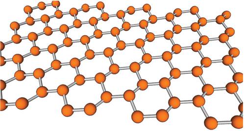
Catalysed by the success of mechanical exfoliated free-standing graphene, two dimensional (2D) semiconductor materials are successively an active area of research. Silicene is a monolayer of silicon (Si) atoms with a low-buckled honeycomb lattice possessing a Dirac cone and massless fermions in the band structure. Another advantage of silicene is its compatibility with the Silicon wafer fabrication technology. To effectively apply this 2D material in the semiconductor industry, it is important to carry out theoretical studies before proceeding to the next step. In this paper, an overview of silicene and silicene nanoribbons (SiNRs) is described. After that, the theoretical studies to engineer the bandgap of silicene are reviewed. Recent theoretical advancement on the applications of silicene for various field-effect transistor (FET) structures is also discussed. Theoretical studies of silicene have shown promising results for their application as FETs and the efforts to study the performance of bandgap-engineered silicene FET should continue to improve the device performance.
中文翻译:
二维蜂窝硅:硅场效应晶体管的理论进展述评
受到机械剥离的自支撑石墨烯的成功的推动,二维(2D)半导体材料已成为一个活跃的研究领域。硅树脂是具有低屈曲蜂窝状晶格的硅(Si)原子的单层,其具有狄拉克锥和能带结构中的无质量费米子。硅的另一个优点是它与硅晶片制造技术的兼容性。为了将这种2D材料有效地应用于半导体行业,在进行下一步之前进行理论研究非常重要。在本文中,对硅和硅纳米带(SiNRs)进行了概述。之后,综述了设计硅带隙的理论研究。还讨论了硅在各种场效应晶体管(FET)结构中的应用的最新理论进展。硅的理论研究显示了其作为FET的应用前景可观的结果,研究带隙工程硅FET的性能的努力应继续改善器件性能。


 京公网安备 11010802027423号