当前位置:
X-MOL 学术
›
Phys. Status Solidi A
›
论文详情
Our official English website, www.x-mol.net, welcomes your
feedback! (Note: you will need to create a separate account there.)
Improved Efficiency of Ultraviolet B Light‐Emitting Diodes with Optimized p‐Side
Physica Status Solidi (A) - Applications and Materials Science Pub Date : 2020-08-19 , DOI: 10.1002/pssa.202000406 Tim Kolbe 1, 2 , Arne Knauer 1 , Jens Rass 1, 2 , Hyun Kyong Cho 1 , Anna Mogilatenko 1, 3 , Sylvia Hagedorn 1 , Neysha Lobo Ploch 1, 2 , Sven Einfeldt 1 , Markus Weyers 1
Physica Status Solidi (A) - Applications and Materials Science Pub Date : 2020-08-19 , DOI: 10.1002/pssa.202000406 Tim Kolbe 1, 2 , Arne Knauer 1 , Jens Rass 1, 2 , Hyun Kyong Cho 1 , Anna Mogilatenko 1, 3 , Sylvia Hagedorn 1 , Neysha Lobo Ploch 1, 2 , Sven Einfeldt 1 , Markus Weyers 1
Affiliation
|
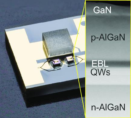
The effects of design and thicknesses of different optically transparent p‐current spreading layers [short‐period superlattice, superlattice (SL), and bulk p‐ ] as well as the type and thickness of the p‐GaN cap layer on the electrical and optical characteristics of 310 nm ultraviolet light‐emitting diodes (LEDs) are investigated. Scanning transmission electron microscopy measurements display self‐organized composition variations in the nonpseudomorphically grown SLs, reducing the effect of increased hole injection efficiency of a SL. In addition, the effect leads to an increased operation voltage. In contrast, the bulk p‐AlGaN layer has a uniform composition and the corresponding LEDs show only a slightly lower output power along with a lower operating voltage. If the thickness of the p‐AlGaN bulk layer in the LED is reduced from 150 nm to 50 nm, the output power increases and the operating voltage decreases. Finally, LEDs with a nonuniform ‐GaN cap layer from a 3D island‐like growth mode feature the highest output power and operating voltage. In contrast, the output power and operating voltage of LEDs with a smooth and closed cap depend on the thickness of ‐GaN. The highest output power and lowest operating voltage are achieved for LEDs with the thinnest ‐GaN cap.
中文翻译:

优化的p侧提高了紫外线B发光二极管的效率
不同光学透明p电流扩展层的设计和厚度的影响[短周期超晶格,超晶格(SL)和体p- ]以及p-GaN盖层的类型和厚度对310 nm紫外发光二极管(LED)的电学和光学特性的影响。扫描透射电子显微镜测量显示非假晶生长的SL中自组织的成分变化,从而减小了SL空穴注入效率提高的影响。另外,该效果导致增加的工作电压。相比之下,体p-AlGaN层具有均匀的组成,相应的LED仅显示出较低的输出功率以及较低的工作电压。如果将LED中的p-AlGaN体层的厚度从150 nm减小到50 nm,则输出功率会增加,工作电压会降低。最后,LED不均匀‐来自3D岛状生长模式的GaN覆盖层具有最高的输出功率和工作电压。相比之下,具有平滑封闭帽的LED的输出功率和工作电压取决于发光二极管的厚度。氮化镓 最薄的LED实现了最高的输出功率和最低的工作电压氮化镓盖。
更新日期:2020-10-22
中文翻译:
优化的p侧提高了紫外线B发光二极管的效率
不同光学透明p电流扩展层的设计和厚度的影响[短周期超晶格,超晶格(SL)和体p- ]以及p-GaN盖层的类型和厚度对310 nm紫外发光二极管(LED)的电学和光学特性的影响。扫描透射电子显微镜测量显示非假晶生长的SL中自组织的成分变化,从而减小了SL空穴注入效率提高的影响。另外,该效果导致增加的工作电压。相比之下,体p-AlGaN层具有均匀的组成,相应的LED仅显示出较低的输出功率以及较低的工作电压。如果将LED中的p-AlGaN体层的厚度从150 nm减小到50 nm,则输出功率会增加,工作电压会降低。最后,LED不均匀‐来自3D岛状生长模式的GaN覆盖层具有最高的输出功率和工作电压。相比之下,具有平滑封闭帽的LED的输出功率和工作电压取决于发光二极管的厚度。氮化镓 最薄的LED实现了最高的输出功率和最低的工作电压氮化镓盖。


 京公网安备 11010802027423号