当前位置:
X-MOL 学术
›
Adv. Eng. Mater.
›
论文详情
Our official English website, www.x-mol.net, welcomes your
feedback! (Note: you will need to create a separate account there.)
Inkjet Printing of Bioresorbable Materials for Manufacturing Transient Microelectronic Devices
Advanced Engineering Materials ( IF 3.4 ) Pub Date : 2020-08-19 , DOI: 10.1002/adem.202000547 Kalyan Y. Mitra 1 , Andreas Willert 1 , Roshan Chandru 2 , Reinhard R. Baumann 1, 2 , Ralf Zichner 1
Advanced Engineering Materials ( IF 3.4 ) Pub Date : 2020-08-19 , DOI: 10.1002/adem.202000547 Kalyan Y. Mitra 1 , Andreas Willert 1 , Roshan Chandru 2 , Reinhard R. Baumann 1, 2 , Ralf Zichner 1
Affiliation
|
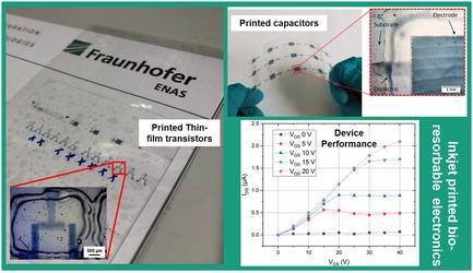
Herein, the inkjet printing of bioresorbable materials tuned to function as electrode, dielectric, and semiconductor layers is reported, thereby developing multilayered microelectronic devices such as capacitors and thin‐film transistors, potentially applicable to address specific medical needs. Polymers and natural materials, e.g., poly(3,4‐ethylenedioxythiophene)‐poly(styrenesulfonate), shellac, and β‐carotene, indigo inks are implemented using jettable formulations, that are either commercially procured or self‐formulated, designed explicitly to deposit fundamental layers for capacitors and transistors. Several parameters are evaluated and adjusted to precisely define a layer's thickness, topology, and geometry, matching with the properties of a fully biodegradable Ormocere substrate, explicitly developed for the specific biological applications. Furthermore, these parameters support in acquiring the intended electrical properties of layers, i.e., conductivity, insulation, semiconductivity, capacitance, and current versus voltage characteristics. The entire manufacturing process of devices is accomplished on the Ormocere substrate under ambient conditions and below 60 °C. The results exhibit that the electrical characteristics of the printed functional layers and devices show direct influence to the physical geometry of the printed features. A fully printed capacitor demonstrates capacitance of 1 nF cm−2, whereas transistors show p‐type and n‐type characteristics with current 0.18–5 μA and mobility 6 × 10⁻⁴–7 × 10⁻² cm2 V−1 s−1.
中文翻译:

用于制造瞬态微电子器件的生物可吸收材料的喷墨印刷
在此,据报道已对生物可吸收材料进行了喷墨印刷,调整后可充当电极,电介质和半导体层,从而开发出了多层微电子器件,例如电容器和薄膜晶体管,有可能适用于满足特定的医疗需求。聚合物和天然材料,例如聚(3,4-亚乙基二氧噻吩)-聚(苯乙烯磺酸盐),虫胶和β-胡萝卜素,靛蓝油墨是使用可喷射配方配制的,可喷射配方是商业采购或自行配制的,专门设计用于沉积电容器和晶体管的基本层。对几个参数进行评估和调整,以精确定义层的厚度,拓扑和几何形状,并与可完全生物降解的Ormocere基材的特性相匹配,为特定的生物学应用而明确开发。此外,这些参数支持获取层的预期电特性,即导电性,绝缘性,半导电性,电容以及电流对电压的特性。器件的整个制造过程均在Ormocere基板上于环境条件和低于60°C的温度下完成。结果表明,印刷功能层和器件的电特性直接影响印刷特征的物理几何形状。完全印刷的电容器的电容为1 nF cm 器件的整个制造过程均在Ormocere基板上于环境条件和低于60°C的温度下完成。结果表明,印刷功能层和器件的电特性直接影响印刷特征的物理几何形状。完全印刷的电容器的电容为1 nF cm 器件的整个制造过程均在Ormocere基板上于环境条件和低于60°C的温度下完成。结果表明,印刷功能层和器件的电特性直接影响印刷特征的物理几何形状。完全印刷的电容器的电容为1 nF cm−2,而晶体管显示p型和n型特性,电流为0.18–5μA,迁移率为6×10 -4 –7×10 -2 cm 2 V -1 s -1。
更新日期:2020-08-19
中文翻译:
用于制造瞬态微电子器件的生物可吸收材料的喷墨印刷
在此,据报道已对生物可吸收材料进行了喷墨印刷,调整后可充当电极,电介质和半导体层,从而开发出了多层微电子器件,例如电容器和薄膜晶体管,有可能适用于满足特定的医疗需求。聚合物和天然材料,例如聚(3,4-亚乙基二氧噻吩)-聚(苯乙烯磺酸盐),虫胶和β-胡萝卜素,靛蓝油墨是使用可喷射配方配制的,可喷射配方是商业采购或自行配制的,专门设计用于沉积电容器和晶体管的基本层。对几个参数进行评估和调整,以精确定义层的厚度,拓扑和几何形状,并与可完全生物降解的Ormocere基材的特性相匹配,为特定的生物学应用而明确开发。此外,这些参数支持获取层的预期电特性,即导电性,绝缘性,半导电性,电容以及电流对电压的特性。器件的整个制造过程均在Ormocere基板上于环境条件和低于60°C的温度下完成。结果表明,印刷功能层和器件的电特性直接影响印刷特征的物理几何形状。完全印刷的电容器的电容为1 nF cm 器件的整个制造过程均在Ormocere基板上于环境条件和低于60°C的温度下完成。结果表明,印刷功能层和器件的电特性直接影响印刷特征的物理几何形状。完全印刷的电容器的电容为1 nF cm 器件的整个制造过程均在Ormocere基板上于环境条件和低于60°C的温度下完成。结果表明,印刷功能层和器件的电特性直接影响印刷特征的物理几何形状。完全印刷的电容器的电容为1 nF cm−2,而晶体管显示p型和n型特性,电流为0.18–5μA,迁移率为6×10 -4 –7×10 -2 cm 2 V -1 s -1。


 京公网安备 11010802027423号