Our official English website, www.x-mol.net, welcomes your
feedback! (Note: you will need to create a separate account there.)
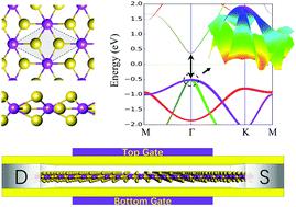
High-performance monolayer Na3Sb shrinking transistors: a DFT-NEGF study.
Nanoscale ( IF 5.8 ) Pub Date : 2020-08-18 , DOI: 10.1039/d0nr04129g Wenhan Zhou 1 , Shengli Zhang , Shiying Guo , Hengze Qu , Bo Cai , Xiang Chen , Haibo Zeng
Nanoscale ( IF 5.8 ) Pub Date : 2020-08-18 , DOI: 10.1039/d0nr04129g Wenhan Zhou 1 , Shengli Zhang , Shiying Guo , Hengze Qu , Bo Cai , Xiang Chen , Haibo Zeng
Affiliation
|
2D materials with direct bandgaps and high carrier mobility are considered excellent candidates for next-generation electronic and optoelectronic devices. Here, a new 2D semiconductor, Na3Sb, is proposed and investigated for the performance limits of FETs by ab initio quantum-transport simulations. Monolayer Na3Sb shows a direct bandgap of 0.89 eV and a high phonon-limited electron mobility of up to 1.25 × 103 cm2 V−1 s−1. We evaluated the impact of channel lengths, gate underlaps, oxide thicknesses, and dielectrics on devices. The major figures of merits for FETs are also assessed in terms of the On–Off ratio, subthreshold swing, gate capacitance, delay time, power dissipation, and field-effect mobility, fulfilling the requirements of the International Roadmap for Devices and Systems (IRDS) for high-performance (HP) devices and demonstrating great potential for electronics with novel 2D Na3Sb.
中文翻译:

高性能单层Na3Sb收缩晶体管:DFT-NEGF研究。
具有直接带隙和高载流子迁移率的2D材料被认为是下一代电子和光电设备的最佳选择。在这里,提出了一种新的2D半导体Na 3 Sb,并通过从头进行量子传输仿真研究了FET的性能极限。单层Na 3 Sb具有0.89 eV的直接带隙和高达1.25×10 3 cm 2 V -1 s -1的高声子极限电子迁移率。我们评估了沟道长度,栅极搭接,氧化物厚度和电介质对器件的影响。FET的主要优点还通过开-关比,亚阈值摆幅,栅极电容,延迟时间,功耗和场效应迁移率进行评估,从而满足《国际设备和系统路线图》(IRDS)的要求)用于高性能(HP)设备,并展示了具有新型2D Na 3 Sb的电子产品的巨大潜力。
更新日期:2020-09-24
中文翻译:
高性能单层Na3Sb收缩晶体管:DFT-NEGF研究。
具有直接带隙和高载流子迁移率的2D材料被认为是下一代电子和光电设备的最佳选择。在这里,提出了一种新的2D半导体Na 3 Sb,并通过从头进行量子传输仿真研究了FET的性能极限。单层Na 3 Sb具有0.89 eV的直接带隙和高达1.25×10 3 cm 2 V -1 s -1的高声子极限电子迁移率。我们评估了沟道长度,栅极搭接,氧化物厚度和电介质对器件的影响。FET的主要优点还通过开-关比,亚阈值摆幅,栅极电容,延迟时间,功耗和场效应迁移率进行评估,从而满足《国际设备和系统路线图》(IRDS)的要求)用于高性能(HP)设备,并展示了具有新型2D Na 3 Sb的电子产品的巨大潜力。


 京公网安备 11010802027423号