当前位置:
X-MOL 学术
›
Adv. Electron. Mater.
›
论文详情
Our official English website, www.x-mol.net, welcomes your
feedback! (Note: you will need to create a separate account there.)
Controlling Defect Formation of Nanoscale AlN: Toward Efficient Current Conduction of Ultrawide‐Bandgap Semiconductors
Advanced Electronic Materials ( IF 5.3 ) Pub Date : 2020-08-17 , DOI: 10.1002/aelm.202000337 Yuanpeng Wu 1 , David A. Laleyan 1 , Zihao Deng 2 , Chihyo Ahn 1 , Anthony F. Aiello 1 , Ayush Pandey 1 , Xianhe Liu 1 , Ping Wang 1 , Kai Sun 2 , Elaheh Ahmadi 1 , Yi Sun 1 , Mackillo Kira 1 , Pallab K. Bhattacharya 1 , Emmanouil Kioupakis 2 , Zetian Mi 1
Advanced Electronic Materials ( IF 5.3 ) Pub Date : 2020-08-17 , DOI: 10.1002/aelm.202000337 Yuanpeng Wu 1 , David A. Laleyan 1 , Zihao Deng 2 , Chihyo Ahn 1 , Anthony F. Aiello 1 , Ayush Pandey 1 , Xianhe Liu 1 , Ping Wang 1 , Kai Sun 2 , Elaheh Ahmadi 1 , Yi Sun 1 , Mackillo Kira 1 , Pallab K. Bhattacharya 1 , Emmanouil Kioupakis 2 , Zetian Mi 1
Affiliation
|
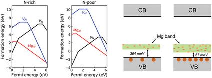
Ultrawide‐bandgap semiconductors such as AlN, BN, and diamond hold tremendous promise for high‐efficiency deep‐ultraviolet optoelectronics and high‐power/frequency electronics, but their practical application has been limited by poor current conduction. Through a combined theoretical and experimental study, it is shown that a critical challenge can be addressed for AlN nanostructures by using N‐rich epitaxy. Under N‐rich conditions, the p‐type Al‐substitutional Mg‐dopant formation energy is significantly reduced by 2 eV, whereas the formation energy for N‐vacancy related compensating defects is increased by ≈3 eV, both of which are essential to achieve high hole concentrations of AlN. Detailed analysis of the current−voltage characteristics of AlN p‐i‐n diodes suggests that current conduction is dominated by hole‐carrier tunneling at room temperature, which is directly related to the activation energy of Mg dopants. At high Mg concentrations, the dispersion of Mg acceptor energy levels leads to drastically reduced activation energy for a portion of Mg dopants, evidenced by the small tunneling energy of 67 meV, which explains the efficient current conduction and the very small turn‐on voltage (≈5 V) for the diodes made of nanoscale AlN. This work shows that nanostructures can overcome the dopability challenges of ultrawide‐bandgap semiconductors and significantly increase the efficiency of devices.
中文翻译:

控制纳米AlN的缺陷形成:实现超宽带隙半导体的有效电流传导
AlN,BN和金刚石等超宽带隙半导体在高效深紫外光电子学和高功率/频率电子学方面具有广阔的前景,但其实际应用受到不良电流传导的限制。通过理论和实验相结合的研究表明,通过使用富氮外延可以解决AlN纳米结构的关键挑战。在富氮条件下,p型Al替代Mg掺杂物的形成能显着降低了2 eV,而与N空位相关的补偿缺陷的形成能增加了约3 eV,这两者对于实现AlN的空穴浓度很高。对AlN p-i-n二极管的电流-电压特性的详细分析表明,在室温下,电流传导主要受空穴-载流子隧穿的影响,这直接与Mg掺杂剂的活化能有关。在高Mg浓度下,Mg受体能级的分散会导致部分Mg掺杂剂的活化能大大降低,这可通过67 meV的小隧穿能来证明,这解释了有效的电流传导和非常小的导通电压(纳米AlN制成的二极管约为≈5 V)。这项工作表明,纳米结构可以克服超宽带隙半导体的掺杂性挑战,并显着提高器件效率。Mg受体能级的分散会导致部分Mg掺杂剂的活化能大大降低,这可通过67 meV的小隧穿能来证明,这说明了有效的电流传导和非常小的导通电压(≈5V)纳米AlN制成的二极管。这项工作表明,纳米结构可以克服超宽带隙半导体的掺杂性挑战,并显着提高器件效率。Mg受体能级的分散会导致部分Mg掺杂剂的活化能大大降低,这可通过67 meV的小隧穿能来证明,这说明了有效的电流传导和非常小的导通电压(≈5V)纳米AlN制成的二极管。这项工作表明,纳米结构可以克服超宽带隙半导体的掺杂挑战,并显着提高器件效率。
更新日期:2020-09-08
中文翻译:
控制纳米AlN的缺陷形成:实现超宽带隙半导体的有效电流传导
AlN,BN和金刚石等超宽带隙半导体在高效深紫外光电子学和高功率/频率电子学方面具有广阔的前景,但其实际应用受到不良电流传导的限制。通过理论和实验相结合的研究表明,通过使用富氮外延可以解决AlN纳米结构的关键挑战。在富氮条件下,p型Al替代Mg掺杂物的形成能显着降低了2 eV,而与N空位相关的补偿缺陷的形成能增加了约3 eV,这两者对于实现AlN的空穴浓度很高。对AlN p-i-n二极管的电流-电压特性的详细分析表明,在室温下,电流传导主要受空穴-载流子隧穿的影响,这直接与Mg掺杂剂的活化能有关。在高Mg浓度下,Mg受体能级的分散会导致部分Mg掺杂剂的活化能大大降低,这可通过67 meV的小隧穿能来证明,这解释了有效的电流传导和非常小的导通电压(纳米AlN制成的二极管约为≈5 V)。这项工作表明,纳米结构可以克服超宽带隙半导体的掺杂性挑战,并显着提高器件效率。Mg受体能级的分散会导致部分Mg掺杂剂的活化能大大降低,这可通过67 meV的小隧穿能来证明,这说明了有效的电流传导和非常小的导通电压(≈5V)纳米AlN制成的二极管。这项工作表明,纳米结构可以克服超宽带隙半导体的掺杂性挑战,并显着提高器件效率。Mg受体能级的分散会导致部分Mg掺杂剂的活化能大大降低,这可通过67 meV的小隧穿能来证明,这说明了有效的电流传导和非常小的导通电压(≈5V)纳米AlN制成的二极管。这项工作表明,纳米结构可以克服超宽带隙半导体的掺杂挑战,并显着提高器件效率。


 京公网安备 11010802027423号