当前位置:
X-MOL 学术
›
ACS Appl. Electron. Mater.
›
论文详情
Our official English website, www.x-mol.net, welcomes your
feedback! (Note: you will need to create a separate account there.)
Organic Thin-Film Transistors with a Bottom Bilayer Gate Dielectric Having a Low Operating Voltage and High Operational Stability
ACS Applied Electronic Materials ( IF 4.3 ) Pub Date : 2020-08-12 , DOI: 10.1021/acsaelm.0c00487 Gunhee Kim 1 , Canek Fuentes-Hernandez 1 , Xiaojia Jia 1 , Bernard Kippelen 1
ACS Applied Electronic Materials ( IF 4.3 ) Pub Date : 2020-08-12 , DOI: 10.1021/acsaelm.0c00487 Gunhee Kim 1 , Canek Fuentes-Hernandez 1 , Xiaojia Jia 1 , Bernard Kippelen 1
Affiliation
|
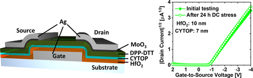
This study reports on p-channel bottom-gate organic thin-film transistors (OTFTs) that achieve low-voltage operation with a thin bilayer gate dielectric of CYTOP/HfO2 that also leads to high operational stability. A bottom-gate geometry allows the thickness of the gate dielectric to be reduced to 17 nm, thereby increasing the gate dielectric capacitance density to a value of up to 258 nF/cm2. All OTFTs yielded threshold voltages (VTH) lower than −1 V, thereby providing a minimum operating voltage (gate to source voltage ∼ VTH) of −1 V with field-effect mobility values in the range 0.3–0.8 cm2/(V s) and subthreshold swing values below 100 mV/dec. Operational stability during DC bias stress was found to be similar to that measured in devices with a top-gate geometry, with about 1% of drain current change after 6 h. Using a double-stretched exponential function, the operational stability characteristics were modeled. It was found that, by increasing the metal oxide layer thickness, the threshold voltage can shift toward positive values under DC stress tests. For CYTOP layer thicknesses above 15 nm, a thicker CYTOP layer was found to shift the threshold voltage in the opposite direction toward negative values. These p-channel bottom-gate organic transistors with a bilayer gate dielectric of CYTOP/HfO2 combine high mobility, high operational stability, and lower voltage operation of −1 V compared to top-gate OTFTs.
中文翻译:

具有双层底栅介质的有机薄膜晶体管,具有低工作电压和高工作稳定性
这项研究报告了p沟道底栅有机薄膜晶体管(OTFT),该薄膜通过CYTOP / HfO 2薄双层栅介质实现了低压操作,这也导致了高操作稳定性。底栅几何形状允许将栅极电介质的厚度减小到17 nm,从而将栅极电介质电容密度增加到高达258 nF / cm 2的值。得到阈值电压(所有的OTFT V TH)比-1V的降低,从而提供的最小操作电压(栅极到源极电压〜V TH)-1 V的场效应迁移率值的范围在0.3-0.8厘米2/(V s)和低于100 mV / dec的亚阈值摆幅值。发现直流偏置应力期间的操作稳定性与具有顶栅几何形状的器件中测得的相似,在6小时后漏极电流变化约为1%。使用双拉伸指数函数,对操作稳定性特征进行了建模。已经发现,通过增加金属氧化物层的厚度,阈值电压可以在直流应力测试下向正值偏移。对于超过15 nm的CYTOP层厚度,发现较厚的CYTOP层会使阈值电压沿相反方向向负值移动。这些具有CYTOP / HfO 2双层栅极电介质的p沟道底栅有机晶体管 与顶栅OTFT相比,具有高迁移率,高操作稳定性和-1 V的低电压操作性能。
更新日期:2020-09-22
中文翻译:
具有双层底栅介质的有机薄膜晶体管,具有低工作电压和高工作稳定性
这项研究报告了p沟道底栅有机薄膜晶体管(OTFT),该薄膜通过CYTOP / HfO 2薄双层栅介质实现了低压操作,这也导致了高操作稳定性。底栅几何形状允许将栅极电介质的厚度减小到17 nm,从而将栅极电介质电容密度增加到高达258 nF / cm 2的值。得到阈值电压(所有的OTFT V TH)比-1V的降低,从而提供的最小操作电压(栅极到源极电压〜V TH)-1 V的场效应迁移率值的范围在0.3-0.8厘米2/(V s)和低于100 mV / dec的亚阈值摆幅值。发现直流偏置应力期间的操作稳定性与具有顶栅几何形状的器件中测得的相似,在6小时后漏极电流变化约为1%。使用双拉伸指数函数,对操作稳定性特征进行了建模。已经发现,通过增加金属氧化物层的厚度,阈值电压可以在直流应力测试下向正值偏移。对于超过15 nm的CYTOP层厚度,发现较厚的CYTOP层会使阈值电压沿相反方向向负值移动。这些具有CYTOP / HfO 2双层栅极电介质的p沟道底栅有机晶体管 与顶栅OTFT相比,具有高迁移率,高操作稳定性和-1 V的低电压操作性能。


 京公网安备 11010802027423号