当前位置:
X-MOL 学术
›
Chem. Mater.
›
论文详情
Our official English website, www.x-mol.net, welcomes your
feedback! (Note: you will need to create a separate account there.)
Microspacing In-Air Sublimation Growth of Ultrathin Organic Single Crystals
Chemistry of Materials ( IF 7.2 ) Pub Date : 2020-08-11 , DOI: 10.1021/acs.chemmater.9b05215 Qing Guo 1 , Xin Ye 1 , Qinglian Lin 1 , Quanxiang Han 1 , Chao Ge 1 , Xiaoxin Zheng 1 , Leilei Zhang 1 , Shuangyue Cui 1 , Yukun Wu 1 , Cuicui Li 1 , Yang Liu 1 , Xutang Tao 1
Chemistry of Materials ( IF 7.2 ) Pub Date : 2020-08-11 , DOI: 10.1021/acs.chemmater.9b05215 Qing Guo 1 , Xin Ye 1 , Qinglian Lin 1 , Quanxiang Han 1 , Chao Ge 1 , Xiaoxin Zheng 1 , Leilei Zhang 1 , Shuangyue Cui 1 , Yukun Wu 1 , Cuicui Li 1 , Yang Liu 1 , Xutang Tao 1
Affiliation
|
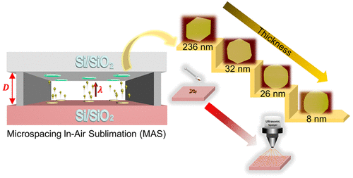
Organic single crystals play indispensable roles in high-performance electronic devices because of their completely eliminated or minimized impurities and disorder, wherein ultrathin thickness is a critical prerequisite because charge accumulation in devices occurs within a few molecular monolayers of the semiconductors. The growth of organic crystals through vapor dispels concerns about solubilities and the inclusion of solvents in the final crystals, but achieving an ultrathin thickness for common organic semiconductors is beyond its power. On the basis of our recently invented microspacing in-air sublimation (MAS), the distance between the source and growth position is set to approximate the mean free path of the vaporized molecules. Such a configuration generates a genetic relationship between the morphology of the source materials and that of the grown crystals. By refining the deposition of the source materials using ultrasonic spray, we can obtain ultrathin single crystals with a uniform distribution. We exemplify the strategy through MAS growth of ultrathin DNTT and pentacene single crystals down to five and three molecular monolayers, respectively. Field effect transistors fabricated on the ultrathin crystals exhibited average charge carrier mobilities of 6.08 cm2 V–1 s–1 for DNTT and 2.39 cm2 V–1 s–1 for pentacene, and low threshold voltages (∼83% of the devices within 5 V).
中文翻译:

超薄有机单晶的微空间空气升华生长
有机单晶由于完全消除或最小化了杂质和无序,因此在高性能电子设备中起着不可或缺的作用,其中超薄厚度是关键的先决条件,因为器件中的电荷积累发生在半导体的几个分子单分子层中。有机晶体通过蒸气的生长消除了人们对最终晶体中的溶解度和溶剂含量的担忧,但是实现普通有机半导体的超薄厚度已超出了其能力范围。根据我们最近发明的微间距空中升华(MAS),将源和生长位置之间的距离设置为近似于汽化分子的平均自由程。这种构型在源材料的形态和生长的晶体的形态之间产生遗传关系。通过使用超声波喷雾细化原始材料的沉积,我们可以获得具有均匀分布的超薄单晶。我们通过MAS生长超薄DNTT和并五苯单晶分别降低到五个和三个分子单层来举例说明该策略。在超薄晶体上制造的场效应晶体管表现出6.08 cm的平均电荷载流子迁移率 分别。在超薄晶体上制造的场效应晶体管表现出6.08 cm的平均电荷载流子迁移率 分别。在超薄晶体上制造的场效应晶体管表现出6.08 cm的平均电荷载流子迁移率2 V -1小号-1为DNTT和2.39厘米2 V -1小号-1为并五苯,和低阈值电压(5 V内的设备的~83%)。
更新日期:2020-09-22
中文翻译:
超薄有机单晶的微空间空气升华生长
有机单晶由于完全消除或最小化了杂质和无序,因此在高性能电子设备中起着不可或缺的作用,其中超薄厚度是关键的先决条件,因为器件中的电荷积累发生在半导体的几个分子单分子层中。有机晶体通过蒸气的生长消除了人们对最终晶体中的溶解度和溶剂含量的担忧,但是实现普通有机半导体的超薄厚度已超出了其能力范围。根据我们最近发明的微间距空中升华(MAS),将源和生长位置之间的距离设置为近似于汽化分子的平均自由程。这种构型在源材料的形态和生长的晶体的形态之间产生遗传关系。通过使用超声波喷雾细化原始材料的沉积,我们可以获得具有均匀分布的超薄单晶。我们通过MAS生长超薄DNTT和并五苯单晶分别降低到五个和三个分子单层来举例说明该策略。在超薄晶体上制造的场效应晶体管表现出6.08 cm的平均电荷载流子迁移率 分别。在超薄晶体上制造的场效应晶体管表现出6.08 cm的平均电荷载流子迁移率 分别。在超薄晶体上制造的场效应晶体管表现出6.08 cm的平均电荷载流子迁移率2 V -1小号-1为DNTT和2.39厘米2 V -1小号-1为并五苯,和低阈值电压(5 V内的设备的~83%)。


 京公网安备 11010802027423号