当前位置:
X-MOL 学术
›
ACS Mater. Lett.
›
论文详情
Our official English website, www.x-mol.net, welcomes your
feedback! (Note: you will need to create a separate account there.)
Structural Phase Transition and Bandgap Control through Mechanical Deformation in Layered Semiconductors 1T–ZrX2 (X = S, Se)
ACS Materials Letters ( IF 9.6 ) Pub Date : 2020-08-04 , DOI: 10.1021/acsmaterialslett.0c00252 Edoardo Martino 1 , David Santos-Cottin 2 , Florian Le Mardelé 2 , Konstantin Semeniuk 1 , Michele Pizzochero 1 , Kristia̅ns Čerņevičs 1 , Benoît Baptiste 3 , Ludovic Delbes 3 , Stefan Klotz 3 , Francesco Capitani 4 , Helmuth Berger 1 , Oleg V. Yazyev 1 , Ana Akrap 2
ACS Materials Letters ( IF 9.6 ) Pub Date : 2020-08-04 , DOI: 10.1021/acsmaterialslett.0c00252 Edoardo Martino 1 , David Santos-Cottin 2 , Florian Le Mardelé 2 , Konstantin Semeniuk 1 , Michele Pizzochero 1 , Kristia̅ns Čerņevičs 1 , Benoît Baptiste 3 , Ludovic Delbes 3 , Stefan Klotz 3 , Francesco Capitani 4 , Helmuth Berger 1 , Oleg V. Yazyev 1 , Ana Akrap 2
Affiliation
|
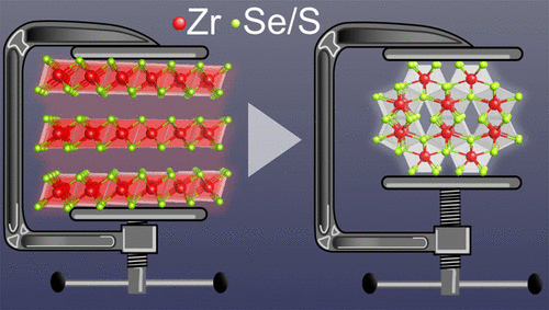
Applying elastic deformation can tune a material’s physical properties locally and reversibly. Spatially modulated lattice deformation can create a bandgap gradient, favoring photogenerated charge separation and collection in optoelectronic devices. These advantages are hindered by the maximum elastic strain that a material can withstand before breaking. Nanomaterials derived by exfoliating transition metal dichalcogenides (TMDs) are an ideal playground for elastic deformation, as they can sustain large elastic strains, up to a few percent. However, exfoliable TMDs with highly strain-tunable properties have proven challenging for researchers to identify. We investigated 1T-ZrS2 and 1T-ZrSe2, exfoliable semiconductors with large bandgaps. Under compressive deformation, both TMDs dramatically change their physical properties. 1T-ZrSe2 undergoes a reversible transformation into an exotic three-dimensional lattice, with a semiconductor-to-metal transition. In ZrS2, the irreversible transformation between two different layered structures is accompanied by a sudden 14% bandgap reduction. These results establish that Zr-based TMDs are an optimal strain-tunable platform for spatially textured bandgaps, with a strong potential for novel optoelectronic devices and light harvesting.
中文翻译:

分层半导体1T–ZrX 2(X = S,Se)中通过机械变形进行结构相变和带隙控制
施加弹性变形可以局部且可逆地调整材料的物理特性。空间调制的晶格变形会产生带隙梯度,从而有利于光电器件中光生电荷的分离和收集。这些优点受到材料在断裂之前可以承受的最大弹性应变的阻碍。通过剥脱过渡金属二硫化碳(TMDs)衍生的纳米材料是弹性变形的理想场所,因为它们可以承受高达百分之几的大弹性应变。但是,事实证明,具有高度应变可调性的可剥脱TMD对研究人员来说具有挑战性。我们研究了1T-ZrS 2和1T-ZrSe 2,具有大带隙的可剥离半导体。在压缩变形下,两个TMD都会显着改变其物理性质。1T-ZrSe 2经过可逆转变为奇异的三维晶格,并具有从半导体到金属的转变。在ZrS 2中,两个不同分层结构之间的不可逆转换伴随着突然的14%带隙减小。这些结果表明,基于Zr的TMD是用于空间纹理化带隙的最佳应变可调平台,在新型光电器件和光收集方面具有强大的潜力。
更新日期:2020-09-08
中文翻译:
分层半导体1T–ZrX 2(X = S,Se)中通过机械变形进行结构相变和带隙控制
施加弹性变形可以局部且可逆地调整材料的物理特性。空间调制的晶格变形会产生带隙梯度,从而有利于光电器件中光生电荷的分离和收集。这些优点受到材料在断裂之前可以承受的最大弹性应变的阻碍。通过剥脱过渡金属二硫化碳(TMDs)衍生的纳米材料是弹性变形的理想场所,因为它们可以承受高达百分之几的大弹性应变。但是,事实证明,具有高度应变可调性的可剥脱TMD对研究人员来说具有挑战性。我们研究了1T-ZrS 2和1T-ZrSe 2,具有大带隙的可剥离半导体。在压缩变形下,两个TMD都会显着改变其物理性质。1T-ZrSe 2经过可逆转变为奇异的三维晶格,并具有从半导体到金属的转变。在ZrS 2中,两个不同分层结构之间的不可逆转换伴随着突然的14%带隙减小。这些结果表明,基于Zr的TMD是用于空间纹理化带隙的最佳应变可调平台,在新型光电器件和光收集方面具有强大的潜力。


 京公网安备 11010802027423号