当前位置:
X-MOL 学术
›
Microelectron. Reliab.
›
论文详情
Our official English website, www.x-mol.net, welcomes your
feedback! (Note: you will need to create a separate account there.)
An ion beam layer removal method of determining the residual stress in the as-fabricated TSV-Cu/TiW/SiO2/Si interface on a nanoscale
Microelectronics Reliability ( IF 1.6 ) Pub Date : 2020-09-01 , DOI: 10.1016/j.microrel.2020.113826 S. Chen , Y.F. En , G.Y. Li , Z.Z. Wang , R. Gao , Rui Ma , L.X. Zhang , Y. Huang
Microelectronics Reliability ( IF 1.6 ) Pub Date : 2020-09-01 , DOI: 10.1016/j.microrel.2020.113826 S. Chen , Y.F. En , G.Y. Li , Z.Z. Wang , R. Gao , Rui Ma , L.X. Zhang , Y. Huang
|
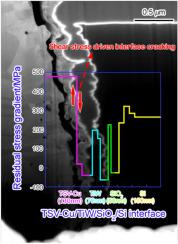
Abstract Thermally induced residual stresses across the TSV-Cu/TiW/SiO2/Si interface in through‑silicon vias (TSVs) have raised serious concerns about mechanical and electrical reliability in 3D ICs. The lack of a nanometer-precision measurement technique for the TSV interfacial stress gradient makes the interface failure mechanism unclear. In this work, we propose an ion beam layer removal (ILR) method for determining the residual stress in the as-fabricated TSV-Cu/TiW/SiO2/Si interface on a nanoscale to facilitate identification of the failure mechanism of the TSV-Cu/TiW/SiO2/Si interface in as-fabricated TSVs. The measurement results showed that the residual stress fluctuates across the TSV-Cu/TiW/SiO2/Si interface and that both compressive stress and tensile stress existed within the interface system. Compressive stress occurred at all three interfaces, the TSV-Cu/TiW, TiW/SiO2, and SiO2/Si interfaces, but transitioned to tensile stress at a distance of 25–45 nm from these interfaces. The highest level of shear stress concentration appeared inside the TSV-Cu at a distance of approximately 45 nm from the TSV-Cu/TiW interface. This shear stress concentration explains the experimentally observed TSV interfacial cracking phenomenon.
中文翻译:

在纳米尺度上确定制造的 TSV-Cu/TiW/SiO2/Si 界面中残余应力的离子束层去除方法
摘要 硅通孔 (TSV) 中 TSV-Cu/TiW/SiO2/Si 界面上的热致残余应力引起了人们对 3D IC 机械和电气可靠性的严重担忧。缺乏针对 TSV 界面应力梯度的纳米级精度测量技术,使得界面失效机制尚不清楚。在这项工作中,我们提出了一种离子束层去除 (ILR) 方法,用于在纳米尺度上确定制造的 TSV-Cu/TiW/SiO2/Si 界面中的残余应力,以促进 TSV-Cu 失效机制的识别制造的 TSV 中的 /TiW/SiO2/Si 界面。测量结果表明,残余应力在 TSV-Cu/TiW/SiO2/Si 界面上发生波动,界面系统内同时存在压应力和拉应力。压应力发生在所有三个界面,即 TSV-Cu/TiW、TiW/SiO2 和 SiO2/Si 界面,但在距离这些界面 25-45 nm 处转变为拉伸应力。最高水平的剪切应力集中出现在距离 TSV-Cu/TiW 界面约 45 nm 处的 TSV-Cu 内部。这种剪切应力集中解释了实验观察到的 TSV 界面开裂现象。
更新日期:2020-09-01
中文翻译:
在纳米尺度上确定制造的 TSV-Cu/TiW/SiO2/Si 界面中残余应力的离子束层去除方法
摘要 硅通孔 (TSV) 中 TSV-Cu/TiW/SiO2/Si 界面上的热致残余应力引起了人们对 3D IC 机械和电气可靠性的严重担忧。缺乏针对 TSV 界面应力梯度的纳米级精度测量技术,使得界面失效机制尚不清楚。在这项工作中,我们提出了一种离子束层去除 (ILR) 方法,用于在纳米尺度上确定制造的 TSV-Cu/TiW/SiO2/Si 界面中的残余应力,以促进 TSV-Cu 失效机制的识别制造的 TSV 中的 /TiW/SiO2/Si 界面。测量结果表明,残余应力在 TSV-Cu/TiW/SiO2/Si 界面上发生波动,界面系统内同时存在压应力和拉应力。压应力发生在所有三个界面,即 TSV-Cu/TiW、TiW/SiO2 和 SiO2/Si 界面,但在距离这些界面 25-45 nm 处转变为拉伸应力。最高水平的剪切应力集中出现在距离 TSV-Cu/TiW 界面约 45 nm 处的 TSV-Cu 内部。这种剪切应力集中解释了实验观察到的 TSV 界面开裂现象。


 京公网安备 11010802027423号