当前位置:
X-MOL 学术
›
J. Mater. Chem. C
›
论文详情
Our official English website, www.x-mol.net, welcomes your
feedback! (Note: you will need to create a separate account there.)
Large-area printed low-voltage organic thin film transistors via minimal-solution bar-coating
Journal of Materials Chemistry C ( IF 5.7 ) Pub Date : 2020-08-04 , DOI: 10.1039/d0tc03089a Sujin Sung 1, 2, 3, 4 , Won-June Lee 1, 2, 3, 4 , Marcia M. Payne 5, 6, 7, 8 , John E. Anthony 5, 6, 7, 8 , Chang-Hyun Kim 4, 9, 10, 11 , Myung-Han Yoon 1, 2, 3, 4
Journal of Materials Chemistry C ( IF 5.7 ) Pub Date : 2020-08-04 , DOI: 10.1039/d0tc03089a Sujin Sung 1, 2, 3, 4 , Won-June Lee 1, 2, 3, 4 , Marcia M. Payne 5, 6, 7, 8 , John E. Anthony 5, 6, 7, 8 , Chang-Hyun Kim 4, 9, 10, 11 , Myung-Han Yoon 1, 2, 3, 4
Affiliation
|
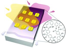
Herein, we report on the fabrication of large-area printed low-voltage organic thin film transistor arrays via minimal-solution bar-coating. We established the bar-coating of the chemically cross-linked polymer dielectric based on poly(4-vinylphenol) and 4,4′-(hexafluoroisopropylidene)diphthalic anhydride by investigating the effects of composition, reaction and printing conditions on film thickness, cross-linking efficacy, and dielectric properties. Subsequently, we elucidated various aspects of large-area (up to 4-inch wafer) bar-coated cross-linked polymeric dielectric prepared from minimal solution (∼100 μL, ∼1.2 μL cm−2) by addressing film uniformity, thickness control, capacitance variation, underlying step coverage, patternability, etc. The resultant polymeric dielectric exhibited good insulating properties as exemplified by a low leakage current density of ∼10−8 A cm−2 (at 1 MV cm−1) and a high areal capacitance of 42.6 nF cm−2. Finally, a highly-crystallized organic semiconductor layer based on 2,8-difluorinated 5,11-bis(triethylsilylethynyl)anthradithiophene was deposited on the bar-coated cross-linked polymeric dielectric via bar-coating, leading to the realization of printed low-voltage organic transistor arrays with minimum ink solution wasted.
中文翻译:

通过最小解决方案的棒涂法大面积印刷低压有机薄膜晶体管
在这里,我们报告通过最小解决方案的棒涂法制造大面积印刷低压有机薄膜晶体管阵列。通过研究组成,反应和印刷条件对膜厚,交联度的影响,我们建立了基于聚(4-乙烯基苯酚)和4,4'-(六氟异亚丙基)二邻苯二甲酸酐的化学交联聚合物电介质的棒涂。链接功效和介电性能。随后,我们通过解决薄膜的均匀性,控制厚度的方法,阐明了由最小溶液(〜100μL,〜1.2μLcm -2)制备的大面积(最多4英寸晶圆)棒状交联聚合物电介质的各个方面。电容变化,潜在的阶跃覆盖范围,可构图性等所得的聚合物电介质表现出良好的绝缘性能,例如〜10 -8 A cm -2的低漏电流密度(在1 MV cm -1处)和42.6 nF cm -2的高面电容。最后,通过棒涂法在棒涂交联的聚合物电介质上沉积了基于2,8-二氟5,11-双(三乙基甲硅烷基乙炔基)蒽噻吩的高度结晶的有机半导体层,从而实现了印刷的浪费最少墨水的高电压有机晶体管阵列。
更新日期:2020-08-04
中文翻译:
通过最小解决方案的棒涂法大面积印刷低压有机薄膜晶体管
在这里,我们报告通过最小解决方案的棒涂法制造大面积印刷低压有机薄膜晶体管阵列。通过研究组成,反应和印刷条件对膜厚,交联度的影响,我们建立了基于聚(4-乙烯基苯酚)和4,4'-(六氟异亚丙基)二邻苯二甲酸酐的化学交联聚合物电介质的棒涂。链接功效和介电性能。随后,我们通过解决薄膜的均匀性,控制厚度的方法,阐明了由最小溶液(〜100μL,〜1.2μLcm -2)制备的大面积(最多4英寸晶圆)棒状交联聚合物电介质的各个方面。电容变化,潜在的阶跃覆盖范围,可构图性等所得的聚合物电介质表现出良好的绝缘性能,例如〜10 -8 A cm -2的低漏电流密度(在1 MV cm -1处)和42.6 nF cm -2的高面电容。最后,通过棒涂法在棒涂交联的聚合物电介质上沉积了基于2,8-二氟5,11-双(三乙基甲硅烷基乙炔基)蒽噻吩的高度结晶的有机半导体层,从而实现了印刷的浪费最少墨水的高电压有机晶体管阵列。


 京公网安备 11010802027423号