当前位置:
X-MOL 学术
›
ACS Photonics
›
论文详情
Our official English website, www.x-mol.net, welcomes your feedback! (Note: you will need to create a separate account there.)
Near Transform-Limited Quantum Dot Linewidths in a Broadband Photonic Crystal Waveguide
ACS Photonics ( IF 7 ) Pub Date : 2020-08-03 , DOI: 10.1021/acsphotonics.0c00758 Freja T. Pedersen 1 , Ying Wang 1 , Cecilie T. Olesen 1 , Sven Scholz 2 , Andreas D. Wieck 2 , Arne Ludwig 2 , Matthias C. Löbl 3 , Richard J. Warburton 3 , Leonardo Midolo 1 , Ravitej Uppu 1 , Peter Lodahl 1
ACS Photonics ( IF 7 ) Pub Date : 2020-08-03 , DOI: 10.1021/acsphotonics.0c00758 Freja T. Pedersen 1 , Ying Wang 1 , Cecilie T. Olesen 1 , Sven Scholz 2 , Andreas D. Wieck 2 , Arne Ludwig 2 , Matthias C. Löbl 3 , Richard J. Warburton 3 , Leonardo Midolo 1 , Ravitej Uppu 1 , Peter Lodahl 1
Affiliation
|
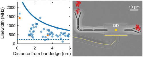
Planar nanophotonic structures enable broadband, near-unity coupling of emission from quantum dots embedded within, thereby realizing ideal single-photon sources. The efficiency and coherence of the single-photon source is limited by charge noise, which results in the broadening of the emission spectrum. We report suppression of the noise by fabricating photonic crystal waveguides in a gallium arsenide membrane containing quantum dots embedded in a p-i-n diode. Local electrical contacts in the vicinity of the waveguides minimize the leakage current and allow fast electrical control (≈4 MHz bandwidth) of the quantum dot resonances. Resonant linewidth measurements of 51 quantum dots coupled to the photonic crystal waveguides exhibit near transform-limited emission over a 6 nm wide range of emission wavelengths. Importantly, the local electrical contacts allow independent tuning of multiple quantum dots on the same chip, which together with the transform-limited emission are key components in realizing multiemitter-based quantum information processing.
中文翻译:

宽带光子晶体波导中接近变换限制的量子点线宽
平面纳米光子结构可实现宽带,嵌入其中的量子点的发射的近统一耦合,从而实现理想的单光子源。单光子源的效率和相干性受到电荷噪声的限制,这导致发射光谱变宽。我们报告通过在砷化镓膜中制造光子晶体波导来抑制噪声,该砷化镓膜中包含嵌入在p - i - n中的量子点二极管。波导附近的局部电触点使泄漏电流最小化,并允许对量子点共振进行快速电控制(≈4MHz带宽)。与光子晶体波导耦合的51个量子点的共振线宽测量结果显示,在6 nm宽的发射波长范围内,发射受限。重要的是,局部电触点允许对同一芯片上的多个量子点进行独立调整,这些量子点与受变换限制的发射一起是实现基于多发射极的量子信息处理的关键组成部分。
更新日期:2020-09-16
中文翻译:
宽带光子晶体波导中接近变换限制的量子点线宽
平面纳米光子结构可实现宽带,嵌入其中的量子点的发射的近统一耦合,从而实现理想的单光子源。单光子源的效率和相干性受到电荷噪声的限制,这导致发射光谱变宽。我们报告通过在砷化镓膜中制造光子晶体波导来抑制噪声,该砷化镓膜中包含嵌入在p - i - n中的量子点二极管。波导附近的局部电触点使泄漏电流最小化,并允许对量子点共振进行快速电控制(≈4MHz带宽)。与光子晶体波导耦合的51个量子点的共振线宽测量结果显示,在6 nm宽的发射波长范围内,发射受限。重要的是,局部电触点允许对同一芯片上的多个量子点进行独立调整,这些量子点与受变换限制的发射一起是实现基于多发射极的量子信息处理的关键组成部分。


 京公网安备 11010802027423号