当前位置:
X-MOL 学术
›
ACS Appl. Electron. Mater.
›
论文详情
Our official English website, www.x-mol.net, welcomes your
feedback! (Note: you will need to create a separate account there.)
Laser-Microstructured ZnO/p-Si Photodetector with Enhanced and Broadband Responsivity across the Ultraviolet–Visible–Near-Infrared Range
ACS Applied Electronic Materials ( IF 4.3 ) Pub Date : 2020-08-03 , DOI: 10.1021/acsaelm.0c00492 Georgios Chatzigiannakis 1, 2 , Angelina Jaros 3 , Renaud Leturcq 4 , Jörgen Jungclaus 3 , Tobias Voss 3 , Spyros Gardelis 2 , Maria Kandyla 1
ACS Applied Electronic Materials ( IF 4.3 ) Pub Date : 2020-08-03 , DOI: 10.1021/acsaelm.0c00492 Georgios Chatzigiannakis 1, 2 , Angelina Jaros 3 , Renaud Leturcq 4 , Jörgen Jungclaus 3 , Tobias Voss 3 , Spyros Gardelis 2 , Maria Kandyla 1
Affiliation
|
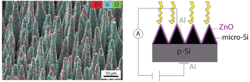
We develop ZnO/p-Si photodetectors by atomic layer deposition (ALD) of ZnO thin films on laser-microstructured silicon, and we investigate their electrical and optical behavior, demonstrating high sensitivity and broadband operation. Microstructured p-type silicon was obtained by nanosecond laser irradiation in SF6 gas, which results in the formation of quasi-ordered and uniform microspikes on the silicon surface. The irradiated silicon contains sulfur impurities, which extend its absorbance to the near-infrared. A thin film of ZnO was conformally deposited on the microstructured silicon substrates by ALD. Photoluminescence measurements indicate high crystalline quality of the ZnO film after annealing. Current–voltage (I−V) measurements of the ZnO/p-Si heterodiodes in the dark show a nonlinear behavior with unusual high current values in reverse bias. Under illumination photocurrent is observed for reverse bias, even for wavelengths below the silicon bandgap in the case of the laser-microstructured photodetectors. Higher current values are measured for the microstructured photodetectors compared to planar ones. Photoconductivity measurements show enhanced responsivity across the UV–vis–NIR spectral range for the laser-microstructured devices because of their increased surface area and light absorption.
中文翻译:

激光微结构化ZnO / p-Si光电探测器,在紫外-可见-近红外范围内具有增强的响应能力和宽带响应能力
我们通过在激光微结构化硅上进行ZnO薄膜的原子层沉积(ALD),开发了ZnO / p-Si光电探测器,并研究了它们的电学和光学行为,证明了其高灵敏度和宽带操作性。通过在SF 6气体中进行纳秒激光辐照获得微结构化的p型硅,这导致在硅表面上形成准有序且均匀的微尖峰。被辐照的硅包含硫杂质,这会将其吸收率扩展到近红外。通过ALD将ZnO薄膜保形地沉积在微结构化的硅基板上。光致发光测量结果表明,退火后ZnO薄膜具有较高的结晶质量。电流电压(I − V)在黑暗中对ZnO / p-Si异质二极管的测量显示出非线性行为,并且反向偏置具有异常高的电流值。在激光微结构化光电探测器的情况下,即使在低于硅带隙的波长下,在光照下也能观察到光电流的反向偏置。与平面型光电探测器相比,微结构光电探测器的电流值更高。光电导率测量结果表明,由于激光微结构化器件的表面积和光吸收增加,它们在整个UV-NIR光谱范围内的响应度得到了增强。
更新日期:2020-09-22
中文翻译:
激光微结构化ZnO / p-Si光电探测器,在紫外-可见-近红外范围内具有增强的响应能力和宽带响应能力
我们通过在激光微结构化硅上进行ZnO薄膜的原子层沉积(ALD),开发了ZnO / p-Si光电探测器,并研究了它们的电学和光学行为,证明了其高灵敏度和宽带操作性。通过在SF 6气体中进行纳秒激光辐照获得微结构化的p型硅,这导致在硅表面上形成准有序且均匀的微尖峰。被辐照的硅包含硫杂质,这会将其吸收率扩展到近红外。通过ALD将ZnO薄膜保形地沉积在微结构化的硅基板上。光致发光测量结果表明,退火后ZnO薄膜具有较高的结晶质量。电流电压(I − V)在黑暗中对ZnO / p-Si异质二极管的测量显示出非线性行为,并且反向偏置具有异常高的电流值。在激光微结构化光电探测器的情况下,即使在低于硅带隙的波长下,在光照下也能观察到光电流的反向偏置。与平面型光电探测器相比,微结构光电探测器的电流值更高。光电导率测量结果表明,由于激光微结构化器件的表面积和光吸收增加,它们在整个UV-NIR光谱范围内的响应度得到了增强。


 京公网安备 11010802027423号