当前位置:
X-MOL 学术
›
Phys. Status Solidi A
›
论文详情
Our official English website, www.x-mol.net, welcomes your feedback! (Note: you will need to create a separate account there.)
A Pathway to Thin GaAs Virtual Substrate on On‐Axis Si (001) with Ultralow Threading Dislocation Density
Physica Status Solidi (A) - Applications and Materials Science ( IF 2 ) Pub Date : 2020-07-25 , DOI: 10.1002/pssa.202000402 Chen Shang 1 , Jennifer Selvidge 1 , Eamonn Hughes 1 , Justin C. Norman 1 , Aidan A. Taylor 1 , Arthur C. Gossard 1 , Kunal Mukherjee 1 , John E. Bowers 1
Physica Status Solidi (A) - Applications and Materials Science ( IF 2 ) Pub Date : 2020-07-25 , DOI: 10.1002/pssa.202000402 Chen Shang 1 , Jennifer Selvidge 1 , Eamonn Hughes 1 , Justin C. Norman 1 , Aidan A. Taylor 1 , Arthur C. Gossard 1 , Kunal Mukherjee 1 , John E. Bowers 1
Affiliation
|
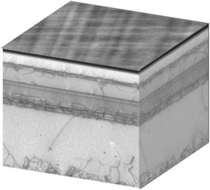
With recent developments in high‐speed and high‐power electronics and Si‐based photonic integration, the concept of monolithic III–V/Si integration through epitaxial methods is gaining momentum. However, the performance and reliability of epitaxially grown devices are still limited by defects in the semiconductor material, especially the threading dislocation density (TDD). Herein, a novel “asymmetric step‐graded filter” structure grown by molecular beam epitaxy (MBE) is proposed based on a systematic study of the commonly used techniques for threading dislocation reduction for high‐quality GaAs on Si (001) growth. The proposed structure greatly enhances the plastic relaxation in the filter layers. A surface TDD lower than 2 × 106 cm−2 is achieved with a total buffer thickness of only 2.55 μm. This provides a clear pathway to further reduce defect density down to the theoretical limit in the 105 cm−2 regime with a thin buffer structure.
中文翻译:

具有超低线程位错密度的同轴Si(001)上薄GaAs虚拟衬底的途径
随着高速和高功率电子学以及基于Si的光子集成的最新发展,通过外延方法进行单片III–V / Si集成的概念日益流行。然而,外延生长的器件的性能和可靠性仍然受到半导体材料中缺陷的限制,特别是螺纹位错密度(TDD)。本文基于分子束外延(MBE)生长的新型“不对称阶梯梯度滤光片”结构,是基于对用于Si(001)生长的高质量GaAs的螺纹位错减少的常用技术的系统研究而提出的。所提出的结构大大增强了过滤层中的塑性松弛。表面TDD低于2×10 6 cm -2使用仅2.55μm的总缓冲厚度即可实现。这提供了一条清晰的途径,可以用薄的缓冲结构将缺陷密度进一步降低到10 5 cm -2范围内的理论极限。
更新日期:2020-07-25
中文翻译:
具有超低线程位错密度的同轴Si(001)上薄GaAs虚拟衬底的途径
随着高速和高功率电子学以及基于Si的光子集成的最新发展,通过外延方法进行单片III–V / Si集成的概念日益流行。然而,外延生长的器件的性能和可靠性仍然受到半导体材料中缺陷的限制,特别是螺纹位错密度(TDD)。本文基于分子束外延(MBE)生长的新型“不对称阶梯梯度滤光片”结构,是基于对用于Si(001)生长的高质量GaAs的螺纹位错减少的常用技术的系统研究而提出的。所提出的结构大大增强了过滤层中的塑性松弛。表面TDD低于2×10 6 cm -2使用仅2.55μm的总缓冲厚度即可实现。这提供了一条清晰的途径,可以用薄的缓冲结构将缺陷密度进一步降低到10 5 cm -2范围内的理论极限。


 京公网安备 11010802027423号