当前位置:
X-MOL 学术
›
Surf. Sci.
›
论文详情
Our official English website, www.x-mol.net, welcomes your
feedback! (Note: you will need to create a separate account there.)
Layer-by-layer control of Ag film growth on Sn/Si(111)−(3×3)−R30∘
Surface Science ( IF 2.1 ) Pub Date : 2020-11-01 , DOI: 10.1016/j.susc.2020.121697 S. Starfelt , R. Lavén , L.S.O. Johansson , H.M. Zhang
Surface Science ( IF 2.1 ) Pub Date : 2020-11-01 , DOI: 10.1016/j.susc.2020.121697 S. Starfelt , R. Lavén , L.S.O. Johansson , H.M. Zhang
|
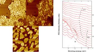
Abstract Silver thin films have been formed on the Sn/Si(111)-( 3 × 3 )-R30∘ surface at room temperature. The film morphologies, growth and electronic structures have been studied by scanning tunneling microscopy/spectroscopy (STM/STS), low-energy electron diffraction (LEED) and angle-resolved photoelectron spectroscopy (ARPES). The first layer of Ag forms an interface which consists of atomic rows with three-fold symmetry oriented along the Si(111)-1 × 1 directions. On top of the interface, Ag grows as an uniform thin film, following a layer-by-layer mode. The electronic structures of the films have been studied by STS for coverages between 1–5 monolayers (MLs). The STS spectra show peaks in the occupied electronic states which move towards the Fermi level with increased film thicknesses. These peaks have been attributed to quantum well states. ARPES measurements have been performed for 1 and 2 ML Ag coverage on Sn/Si(111)-( 3 × 3 )-R30∘, where the resulting thicknesses were confirmed by STM. The spectra reveal that quantum well states appear first for the 2 ML film.
中文翻译:

Sn/Si(111)-(3×3)-R30∘上Ag薄膜生长的逐层控制
摘要 室温下在 Sn/Si(111)-( 3 × 3 )-R30∘ 表面形成了银薄膜。通过扫描隧道显微镜/光谱(STM/STS)、低能电子衍射(LEED)和角分辨光电子能谱(ARPES)研究了薄膜的形态、生长和电子结构。第一层 Ag 形成一个界面,该界面由沿 Si(111)-1 × 1 方向定向的具有三重对称性的原子行组成。在界面顶部,Ag 以逐层模式生长为均匀的薄膜。STS 已经研究了薄膜的电子结构,以覆盖 1-5 个单层 (ML)。STS 光谱显示占据电子态的峰值随着膜厚度的增加而向费米能级移动。这些峰归因于量子阱态。已经对 Sn/Si(111)-( 3 × 3 )-R30∘ 上的 1 和 2 ML Ag 覆盖率进行了 ARPES 测量,其中得到的厚度由 STM 确认。光谱显示量子阱态首先出现在 2 ML 薄膜中。
更新日期:2020-11-01
中文翻译:
Sn/Si(111)-(3×3)-R30∘上Ag薄膜生长的逐层控制
摘要 室温下在 Sn/Si(111)-( 3 × 3 )-R30∘ 表面形成了银薄膜。通过扫描隧道显微镜/光谱(STM/STS)、低能电子衍射(LEED)和角分辨光电子能谱(ARPES)研究了薄膜的形态、生长和电子结构。第一层 Ag 形成一个界面,该界面由沿 Si(111)-1 × 1 方向定向的具有三重对称性的原子行组成。在界面顶部,Ag 以逐层模式生长为均匀的薄膜。STS 已经研究了薄膜的电子结构,以覆盖 1-5 个单层 (ML)。STS 光谱显示占据电子态的峰值随着膜厚度的增加而向费米能级移动。这些峰归因于量子阱态。已经对 Sn/Si(111)-( 3 × 3 )-R30∘ 上的 1 和 2 ML Ag 覆盖率进行了 ARPES 测量,其中得到的厚度由 STM 确认。光谱显示量子阱态首先出现在 2 ML 薄膜中。


 京公网安备 11010802027423号