当前位置:
X-MOL 学术
›
Adv. Mater.
›
论文详情
Our official English website, www.x-mol.net, welcomes your feedback! (Note: you will need to create a separate account there.)
Wafer-Scale High-Quality Microtubular Devices Fabricated via Dry-Etching for Optical and Microelectronic Applications.
Advanced Materials ( IF 29.4 ) Pub Date : 2020-07-19 , DOI: 10.1002/adma.202003252 Christian N Saggau 1 , Felix Gabler 1, 2 , Dmitriy D Karnaushenko 1 , Daniil Karnaushenko 1 , Libo Ma 1 , Oliver G Schmidt 1, 2, 3
Advanced Materials ( IF 29.4 ) Pub Date : 2020-07-19 , DOI: 10.1002/adma.202003252 Christian N Saggau 1 , Felix Gabler 1, 2 , Dmitriy D Karnaushenko 1 , Daniil Karnaushenko 1 , Libo Ma 1 , Oliver G Schmidt 1, 2, 3
Affiliation
|
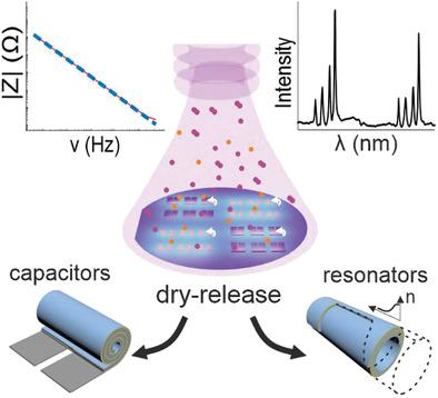
Mechanical strain formed at the interfaces of thin films has been widely applied to self‐assemble 3D microarchitectures. Among them, rolled‐up microtubes possess a unique 3D geometry beneficial for working as photonic, electromagnetic, energy storage, and sensing devices. However, the yield and quality of microtubular architectures are often limited by the wet‐release of lithographically patterned stacks of thin‐film structures. To address the drawbacks of conventionally used wet‐etching methods in self‐assembly techniques, here a dry‐release approach is developed to roll‐up both metallic and dielectric, as well as metallic/dielectric hybrid thin films for the fabrication of electronic and optical devices. A silicon thin film sacrificial layer on insulator is etched by dry fluorine chemistry, triggering self‐assembly of prestrained nanomembranes in a well‐controlled wafer scale fashion. More than 6000 integrated microcapacitors as well as hundreds of active microtubular optical cavities are obtained in a simultaneous self‐assembly process. The fabrication of wafer‐scale self‐assembled microdevices results in high yield, reproducibility, uniformity, and performance, which promise broad applications in microelectronics, photonics, and opto‐electronics.
中文翻译:

通过干蚀刻制造的用于光学和微电子应用的晶圆级高质量微管器件。
薄膜界面处形成的机械应变已广泛应用于自组装3D微体系结构。其中,卷起的微管具有独特的3D几何形状,非常适合用作光子,电磁,能量存储和传感设备。但是,微管结构的产量和质量通常受到湿法释放薄膜结构的平版印刷图案堆叠的限制。为了解决自组装技术中常规使用的湿法刻蚀方法的缺陷,这里开发了一种干法剥离方法,可将金属和电介质以及金属/电介质混合薄膜卷起来,以制造电子和光学材料。设备。绝缘体上的硅薄膜牺牲层通过干氟化学蚀刻,以良好的晶圆尺寸控制方式触发预应变纳米膜的自组装。在同时的自组装过程中,获得了6000多个集成式微电容器以及数百个有源微管光学腔。晶圆级自组装微器件的制造带来了高产量,可重复性,均匀性和高性能,有望在微电子,光子学和光电领域得到广泛的应用。
更新日期:2020-09-15
中文翻译:
通过干蚀刻制造的用于光学和微电子应用的晶圆级高质量微管器件。
薄膜界面处形成的机械应变已广泛应用于自组装3D微体系结构。其中,卷起的微管具有独特的3D几何形状,非常适合用作光子,电磁,能量存储和传感设备。但是,微管结构的产量和质量通常受到湿法释放薄膜结构的平版印刷图案堆叠的限制。为了解决自组装技术中常规使用的湿法刻蚀方法的缺陷,这里开发了一种干法剥离方法,可将金属和电介质以及金属/电介质混合薄膜卷起来,以制造电子和光学材料。设备。绝缘体上的硅薄膜牺牲层通过干氟化学蚀刻,以良好的晶圆尺寸控制方式触发预应变纳米膜的自组装。在同时的自组装过程中,获得了6000多个集成式微电容器以及数百个有源微管光学腔。晶圆级自组装微器件的制造带来了高产量,可重复性,均匀性和高性能,有望在微电子,光子学和光电领域得到广泛的应用。


 京公网安备 11010802027423号