当前位置:
X-MOL 学术
›
Microelectron. Eng.
›
论文详情
Our official English website, www.x-mol.net, welcomes your feedback! (Note: you will need to create a separate account there.)
Mechanisms of GaAs surface passivation by a one-step dry process using low-frequency plasma enhanced chemical deposition of silicon nitride
Microelectronic Engineering ( IF 2.3 ) Pub Date : 2020-09-01 , DOI: 10.1016/j.mee.2020.111398 Olivier Richard , Sonia Blais , Richard Arès , Vincent Aimez , Abdelatif Jaouad
Microelectronic Engineering ( IF 2.3 ) Pub Date : 2020-09-01 , DOI: 10.1016/j.mee.2020.111398 Olivier Richard , Sonia Blais , Richard Arès , Vincent Aimez , Abdelatif Jaouad
|
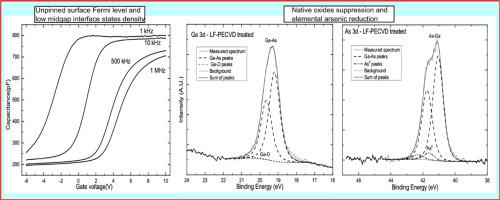
Abstract III-V materials are known for their high surface states densities which degrade the performances of photonic and electronic devices. Plasma-enhanced chemical vapor deposition of SixNy is commonly used to passivate surface states and to encapsulate III-V devices and circuits. The plasma is generated with an RF excitation source usually set at a high frequency of 13.56 MHz. To obtain a high quality III-V/SixNy interface, many chemical surface treatments are required before deposition, as well as post-deposition thermal annealing. In this work, we demonstrate that a low-frequency plasma allows for an efficient passivation process by a simple deposition of SixNy, without any wet chemical pretreatment nor post-deposition annealing. This dry process is more compatible with the passivation and encapsulation of completed III-V devices and circuits. Metal-insulator-semiconductor capacitors were fabricated by depositing SixNy on GaAs at a frequency of 90 kHz. C V measurements indicated the unpinning of the Fermi level and a low density of surface states in the mid 1011 cm−2 eV−1 range. X-ray photoelectron spectra have shown the complete suppression of native oxides and an important reduction of elemental arsenic from the GaAs surface. The mechanisms of surface passivation by ionic hydrogen bombardment inherent to the low-frequency plasma deposition of SixNy are discussed.
中文翻译:

使用低频等离子体增强氮化硅化学沉积的一步干法钝化 GaAs 表面的机制
摘要 III-V 族材料以其高表面态密度而闻名,这会降低光子和电子器件的性能。SixNy 的等离子体增强化学气相沉积通常用于钝化表面状态和封装 III-V 器件和电路。等离子体由通常设置为 13.56 MHz 高频的 RF 激发源产生。为了获得高质量的 III-V/SixNy 界面,需要在沉积前进行许多化学表面处理,以及沉积后热退火。在这项工作中,我们证明了低频等离子体可以通过简单的 SixNy 沉积实现有效的钝化过程,无需任何湿化学预处理或沉积后退火。这种干式工艺更适合完整的 III-V 族器件和电路的钝化和封装。通过在 GaAs 上以 90 kHz 的频率沉积 SixNy 来制造金属-绝缘体-半导体电容器。CV 测量表明费米能级的非钉扎和 1011 cm-2 eV-1 中间范围内的低表面态密度。X 射线光电子能谱显示完全抑制了天然氧化物,并显着减少了 GaAs 表面的元素砷。讨论了 SixNy 低频等离子体沉积固有的离子氢轰击表面钝化的机制。CV 测量表明费米能级的非钉扎和 1011 cm-2 eV-1 中间范围内的低表面态密度。X 射线光电子能谱显示完全抑制了天然氧化物,并显着减少了 GaAs 表面的元素砷。讨论了 SixNy 低频等离子体沉积固有的离子氢轰击表面钝化的机制。CV 测量表明费米能级的非钉扎和 1011 cm-2 eV-1 中间范围内的低表面态密度。X 射线光电子能谱显示出对天然氧化物的完全抑制和 GaAs 表面元素砷的重要减少。讨论了 SixNy 低频等离子体沉积固有的离子氢轰击表面钝化的机制。
更新日期:2020-09-01
中文翻译:
使用低频等离子体增强氮化硅化学沉积的一步干法钝化 GaAs 表面的机制
摘要 III-V 族材料以其高表面态密度而闻名,这会降低光子和电子器件的性能。SixNy 的等离子体增强化学气相沉积通常用于钝化表面状态和封装 III-V 器件和电路。等离子体由通常设置为 13.56 MHz 高频的 RF 激发源产生。为了获得高质量的 III-V/SixNy 界面,需要在沉积前进行许多化学表面处理,以及沉积后热退火。在这项工作中,我们证明了低频等离子体可以通过简单的 SixNy 沉积实现有效的钝化过程,无需任何湿化学预处理或沉积后退火。这种干式工艺更适合完整的 III-V 族器件和电路的钝化和封装。通过在 GaAs 上以 90 kHz 的频率沉积 SixNy 来制造金属-绝缘体-半导体电容器。CV 测量表明费米能级的非钉扎和 1011 cm-2 eV-1 中间范围内的低表面态密度。X 射线光电子能谱显示完全抑制了天然氧化物,并显着减少了 GaAs 表面的元素砷。讨论了 SixNy 低频等离子体沉积固有的离子氢轰击表面钝化的机制。CV 测量表明费米能级的非钉扎和 1011 cm-2 eV-1 中间范围内的低表面态密度。X 射线光电子能谱显示完全抑制了天然氧化物,并显着减少了 GaAs 表面的元素砷。讨论了 SixNy 低频等离子体沉积固有的离子氢轰击表面钝化的机制。CV 测量表明费米能级的非钉扎和 1011 cm-2 eV-1 中间范围内的低表面态密度。X 射线光电子能谱显示出对天然氧化物的完全抑制和 GaAs 表面元素砷的重要减少。讨论了 SixNy 低频等离子体沉积固有的离子氢轰击表面钝化的机制。


 京公网安备 11010802027423号