当前位置:
X-MOL 学术
›
ACS Appl. Electron. Mater.
›
论文详情
Our official English website, www.x-mol.net, welcomes your
feedback! (Note: you will need to create a separate account there.)
Switching Behavior in a Vertical Tunneling Transistor by Tunneling Mechanism Transition and Floating Electrode Structure
ACS Applied Electronic Materials ( IF 4.3 ) Pub Date : 2020-07-10 , DOI: 10.1021/acsaelm.0c00409 Jeong Hee Shin 1 , Su Jin Heo 1 , Jae Hoon Yang 1 , Hyun Sik Kim 2 , Jae Eun Jung 3 , Hyuk-Jun Kwon 1 , Jae Eun Jang 1
ACS Applied Electronic Materials ( IF 4.3 ) Pub Date : 2020-07-10 , DOI: 10.1021/acsaelm.0c00409 Jeong Hee Shin 1 , Su Jin Heo 1 , Jae Hoon Yang 1 , Hyun Sik Kim 2 , Jae Eun Jung 3 , Hyuk-Jun Kwon 1 , Jae Eun Jang 1
Affiliation
|
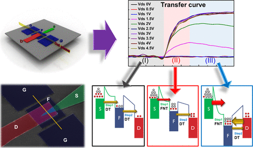
Direct application of the tunneling mechanism into the conventional field-effect transistor structure only results in inefficient switching behavior and high leakage current. Here, we report a vertical metal–insulator–metal (MIM) tunneling transistor employing a floating electrode to achieve an efficient switching behavior and substantially low leakage current simultaneously. This switching method utilizes a tunneling mechanism transition between direct and Fowler–Nordheim tunneling by placing the floating electrode into a vertical tunneling channel. Engineering the electrical potential of the floating electrode with coplanar dual gates enables the efficient control of the tunneling mechanism transition. This particular arrangement of the gate and source/drain (no overlap) allows an extremely low gate leakage current (∼10–13 A). This value is significant in the tunneling transistor and promising for future electrical devices with low-power consumption. Furthermore, tunneling, whose operating principle is fundamentally different from the p–n junction and Schottky barrier in the Si transistor, has been proposed as a solution to tackle the issues such as high-frequency driving, power consumption, and so on. This structure is a strong candidate for ultrahigh-frequency driving because of its extremely low structural capacitance (∼1.5 zF). An additional electrical status can be shown to generate ternary or more statuses in a single transistor. Its electrical performance is expected to not only harmonize with THz communication systems, control process units, and high-speed electrical systems but also contributes a degree of integration. Moreover, the simple and low-temperature fabrication process of the vertical MIM tunneling transistor is advantageous for low-cost electrical devices and flexible electronic applications.
中文翻译:

垂直隧穿晶体管的隧穿机制转换和浮动电极结构的开关特性
将隧穿机制直接应用到常规场效应晶体管结构中只会导致无效的开关行为和高漏电流。在这里,我们报道了一种采用浮置电极的垂直金属-绝缘体-金属(MIM)隧道晶体管,可同时实现有效的开关性能和低泄漏电流。这种转换方法通过将浮动电极置于垂直隧穿通道中,从而在直接隧穿和Fowler-Nordheim隧穿之间利用隧穿机制进行转换。用共面双栅极设计浮动电极的电势可以有效控制隧穿机制的转变。栅极和源极/漏极的这种特殊布置(无重叠)允许极低的栅极泄漏电流(〜10–13一种)。该值在隧道晶体管中非常重要,并有望用于未来的低功耗电子设备。此外,已经提出了隧穿作为解决高频驱动,功耗等问题的解决方案,其工作原理与Si晶体管中的p–n结和肖特基势垒根本不同。由于其极低的结构电容(〜1.5 zF),该结构非常适合用于超高频驱动。可以显示其他电气状态,以在单个晶体管中生成三态或更多状态。预期其电气性能不仅可以与THz通信系统,控制处理单元和高速电气系统相协调,而且可以提高集成度。此外,
更新日期:2020-08-25
中文翻译:
垂直隧穿晶体管的隧穿机制转换和浮动电极结构的开关特性
将隧穿机制直接应用到常规场效应晶体管结构中只会导致无效的开关行为和高漏电流。在这里,我们报道了一种采用浮置电极的垂直金属-绝缘体-金属(MIM)隧道晶体管,可同时实现有效的开关性能和低泄漏电流。这种转换方法通过将浮动电极置于垂直隧穿通道中,从而在直接隧穿和Fowler-Nordheim隧穿之间利用隧穿机制进行转换。用共面双栅极设计浮动电极的电势可以有效控制隧穿机制的转变。栅极和源极/漏极的这种特殊布置(无重叠)允许极低的栅极泄漏电流(〜10–13一种)。该值在隧道晶体管中非常重要,并有望用于未来的低功耗电子设备。此外,已经提出了隧穿作为解决高频驱动,功耗等问题的解决方案,其工作原理与Si晶体管中的p–n结和肖特基势垒根本不同。由于其极低的结构电容(〜1.5 zF),该结构非常适合用于超高频驱动。可以显示其他电气状态,以在单个晶体管中生成三态或更多状态。预期其电气性能不仅可以与THz通信系统,控制处理单元和高速电气系统相协调,而且可以提高集成度。此外,


 京公网安备 11010802027423号