当前位置:
X-MOL 学术
›
Microelectron. Eng.
›
论文详情
Our official English website, www.x-mol.net, welcomes your
feedback! (Note: you will need to create a separate account there.)
Vertical MOS and tunnel FETs in the same silicon pillar structure with Al and TiN gate electrodes
Microelectronic Engineering ( IF 2.6 ) Pub Date : 2020-07-01 , DOI: 10.1016/j.mee.2020.111399 Luís F. Pinotti , Frederico H. Cioldin , Alfredo R. Vaz , Luana C.J. Espíndola , José A. Diniz
Microelectronic Engineering ( IF 2.6 ) Pub Date : 2020-07-01 , DOI: 10.1016/j.mee.2020.111399 Luís F. Pinotti , Frederico H. Cioldin , Alfredo R. Vaz , Luana C.J. Espíndola , José A. Diniz
|
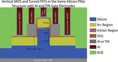
Abstract This work presents a silicon pillar structure containing both MOS (Metal-Oxide-Semiconductor) and Tunnel Field Effect Transistors (MOSFETs and TFETs, respectively) with Al and TiN double-gate electrodes. The abrupt n+ regions of drain/source in the p-Si vertical pillar are obtained from sequential 31P+ ion implantations (energies of 100, 50 and 25 keV) and Rapid Thermal Annealing (RTA). The abrupt drain region in the p-Si pillar allows the vertical control of the channel length of the MOSFET device (achieving lengths such as 70 nm) and the formation of a nano-intrinsic region (2 nm), between n+ and p regions, fundamental for the operation of a TFET. The MOSFETs and TFETs, which were fabricated with Al gate, have presented the better results (Ion of 56 μA/μm, gm of 45 μS/μm and (Ion/Ioff) ratio of 107) related to higher performance in conduction regime. However, both devices, fabricated with TiN, have presented higher performance related to leakage and/or off current (Ioff of 1.8 pA/μm). It is important to notice that the alternating use at the same silicon pillar for the both MOSFET or TFET devices can be suitable to the applications in which are necessary high and low power operations, respectively.
中文翻译:

具有 Al 和 TiN 栅电极的同一硅柱结构中的垂直 MOS 和隧道 FET
摘要 这项工作提出了一种包含 MOS(金属氧化物半导体)和隧道场效应晶体管(分别为 MOSFET 和 TFET)的硅柱结构,具有 Al 和 TiN 双栅电极。p-Si 垂直柱中漏极/源极的突变 n+ 区是通过连续的 31P+ 离子注入(能量为 100、50 和 25 keV)和快速热退火 (RTA) 获得的。p-Si 柱中的陡峭漏区允许垂直控制 MOSFET 器件的沟道长度(达到 70 nm 等长度),并在 n+ 和 p 区之间形成纳米本征区(2 nm), TFET 操作的基础。用 Al 栅极制造的 MOSFET 和 TFET 表现出更好的结果(离子为 56 μA/μm,45 μS/μm 的 gm 和 107 的 (Ion/Ioff) 比值)与更高的导电性能相关。然而,这两种用 TiN 制造的器件在漏电流和/或关断电流(Ioff 为 1.8 pA/μm)方面表现出更高的性能。需要注意的是,MOSFET 或 TFET 器件在同一硅柱上交替使用可以分别适用于需要高功率和低功率操作的应用,这一点很重要。
更新日期:2020-07-01
中文翻译:
具有 Al 和 TiN 栅电极的同一硅柱结构中的垂直 MOS 和隧道 FET
摘要 这项工作提出了一种包含 MOS(金属氧化物半导体)和隧道场效应晶体管(分别为 MOSFET 和 TFET)的硅柱结构,具有 Al 和 TiN 双栅电极。p-Si 垂直柱中漏极/源极的突变 n+ 区是通过连续的 31P+ 离子注入(能量为 100、50 和 25 keV)和快速热退火 (RTA) 获得的。p-Si 柱中的陡峭漏区允许垂直控制 MOSFET 器件的沟道长度(达到 70 nm 等长度),并在 n+ 和 p 区之间形成纳米本征区(2 nm), TFET 操作的基础。用 Al 栅极制造的 MOSFET 和 TFET 表现出更好的结果(离子为 56 μA/μm,45 μS/μm 的 gm 和 107 的 (Ion/Ioff) 比值)与更高的导电性能相关。然而,这两种用 TiN 制造的器件在漏电流和/或关断电流(Ioff 为 1.8 pA/μm)方面表现出更高的性能。需要注意的是,MOSFET 或 TFET 器件在同一硅柱上交替使用可以分别适用于需要高功率和低功率操作的应用,这一点很重要。


 京公网安备 11010802027423号