当前位置:
X-MOL 学术
›
J. Am. Chem. Soc.
›
论文详情
Our official English website, www.x-mol.net, welcomes your
feedback! (Note: you will need to create a separate account there.)
Bottom-up Assembly of Nanoporous Graphene with Emergent Electronic States
Journal of the American Chemical Society ( IF 14.4 ) Pub Date : 2020-07-09 , DOI: 10.1021/jacs.0c05235 Peter H Jacobse 1 , Ryan D McCurdy 2 , Jingwei Jiang 1 , Daniel J Rizzo 1 , Gregory Veber 2 , Paul Butler 1 , Rafał Zuzak 1, 3 , Steven G Louie 1, 4 , Felix R Fischer 2, 4, 5 , Michael F Crommie 1, 4, 5
Journal of the American Chemical Society ( IF 14.4 ) Pub Date : 2020-07-09 , DOI: 10.1021/jacs.0c05235 Peter H Jacobse 1 , Ryan D McCurdy 2 , Jingwei Jiang 1 , Daniel J Rizzo 1 , Gregory Veber 2 , Paul Butler 1 , Rafał Zuzak 1, 3 , Steven G Louie 1, 4 , Felix R Fischer 2, 4, 5 , Michael F Crommie 1, 4, 5
Affiliation
|
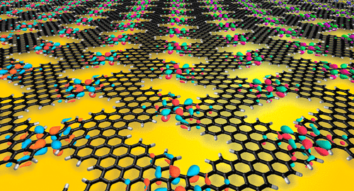
The incorporation of nanoscale pores into a sheet of graphene allows it to switch from an impermeable semimetal to a semiconducting nano-sieve. Nanoporous graphenes are desirable for applications ranging from high-performance semiconductor device channels to atomically-thin molecular sieve membranes, and their performance is highly dependent on the periodicity and reproducibility of pores at the atomic level. Achieving precise nanopore topologies in graphene using top-down lithographic approaches has proven to be challenging due to poor structural control at the atomic level. Alternatively, atomically-precise nanometer-sized pores can be fabricated via lateral fusion of bottom-up synthesized graphene nanoribbons. This technique, however, typically requires an additional high temperature cross-coupling step following the nanoribbon formation that inherently yields poor lateral conjugation, resulting in 2D materials that are weakly connected both mechanically and electronically. Here we demonstrate a novel bottom-up approach for forming fully conjugated nanoporous graphene through a single, mild annealing step following the initial polymer formation. We find emergent interface-localized electronic states within the bulk band gap of the graphene nanoribbon that hybridize to yield a dispersive two-dimensional low-energy band of states. We show that this low-energy band can be rationalized in terms of edge states of the constituent single-strand nanoribbons. The localization of these 2D states around pores makes this material particularly attractive for applications requiring electronically sensitive molecular sieves.
中文翻译:

自下而上组装纳米多孔石墨烯与电子状态
将纳米级孔纳入石墨烯片中,使其能够从不透水的半金属转变为半导体纳米筛。纳米多孔石墨烯适用于从高性能半导体器件通道到原子级薄分子筛膜的应用,其性能高度依赖于原子级孔隙的周期性和再现性。由于原子水平的结构控制不佳,使用自上而下的光刻方法在石墨烯中实现精确的纳米孔拓扑结构已被证明具有挑战性。或者,可以通过自下而上合成的石墨烯纳米带的横向融合来制造原子级精确的纳米级孔。然而这种技术,通常需要在纳米带形成后进行额外的高温交叉耦合步骤,这本身就会产生不良的横向共轭,从而导致二维材料在机械和电子方面的连接都很弱。在这里,我们展示了一种新的自下而上的方法,用于在初始聚合物形成后通过单个温和的退火步骤形成完全共轭纳米多孔石墨烯。我们在石墨烯纳米带的体带隙内发现了突现的界面局部电子态,这些电子态杂化产生分散的二维低能带。我们表明,该低能带可以根据组成单链纳米带的边缘状态进行合理化。
更新日期:2020-07-09
中文翻译:
自下而上组装纳米多孔石墨烯与电子状态
将纳米级孔纳入石墨烯片中,使其能够从不透水的半金属转变为半导体纳米筛。纳米多孔石墨烯适用于从高性能半导体器件通道到原子级薄分子筛膜的应用,其性能高度依赖于原子级孔隙的周期性和再现性。由于原子水平的结构控制不佳,使用自上而下的光刻方法在石墨烯中实现精确的纳米孔拓扑结构已被证明具有挑战性。或者,可以通过自下而上合成的石墨烯纳米带的横向融合来制造原子级精确的纳米级孔。然而这种技术,通常需要在纳米带形成后进行额外的高温交叉耦合步骤,这本身就会产生不良的横向共轭,从而导致二维材料在机械和电子方面的连接都很弱。在这里,我们展示了一种新的自下而上的方法,用于在初始聚合物形成后通过单个温和的退火步骤形成完全共轭纳米多孔石墨烯。我们在石墨烯纳米带的体带隙内发现了突现的界面局部电子态,这些电子态杂化产生分散的二维低能带。我们表明,该低能带可以根据组成单链纳米带的边缘状态进行合理化。


 京公网安备 11010802027423号