当前位置:
X-MOL 学术
›
Appl. Surf. Sci.
›
论文详情
Our official English website, www.x-mol.net, welcomes your
feedback! (Note: you will need to create a separate account there.)
Filamentary and interface switching of CMOS-compatible Ta2O5 memristor for non-volatile memory and synaptic devices
Applied Surface Science ( IF 6.3 ) Pub Date : 2020-11-01 , DOI: 10.1016/j.apsusc.2020.147167 Ji-Ho Ryu , Fayyaz Hussain , Chandreswar Mahata , Muhammad Ismail , Yawar Abbas , Min-Hwi Kim , Changhwan Choi , Byung-Gook Park , Sungjun Kim
Applied Surface Science ( IF 6.3 ) Pub Date : 2020-11-01 , DOI: 10.1016/j.apsusc.2020.147167 Ji-Ho Ryu , Fayyaz Hussain , Chandreswar Mahata , Muhammad Ismail , Yawar Abbas , Min-Hwi Kim , Changhwan Choi , Byung-Gook Park , Sungjun Kim
|
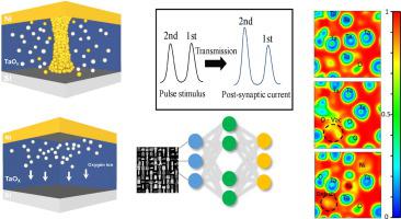
Abstract To successively implement synaptic memristor device in the neuromorphic computing system, it is essential to perform a variety of synaptic characteristics with low power consumption and have complementary metal-oxidesemiconductor (CMOS) compatibility. In this work, we experimentally demonstrate two types of interface and filamentary resistive switching behaviors for Ni/Ta2O5/Si device by controlling electroforming process. The typical bipolar operation with filamentary switching is observed with electroforming for non-volatile memory properties such as reliable retention (>104) and high on/off ratio (>103). To achieve the synaptic characteristics such as paired pulse facilitation (PPF), potentiation, and depression, the gradual switching with low current without electroforming is used. We evaluate pattern recognition accuracy simulation from Fashion MNIST dataset by using a 3-layer neural network (784 × 512 × 10) and synaptic weight of Ni/Ta2O5/Si device. Furthermore, density of states, isosurface charge density and electron localization function plots confirm the conductivity and charge formation of Ta2O5 structure with and without oxygen vacancies. Theoretical work results reveal that the resistive switching characteristics are due to charge accumulation/depletion near the defects sites (oxygen vacancy). All things considered, the Ni/Ta2O5/p++-Si memristor could offer the flexibility for both non-volatile memory and synaptic devices by simply controlling electroforming.
中文翻译:

用于非易失性存储器和突触器件的 CMOS 兼容 Ta2O5 忆阻器的丝状和接口切换
摘要 要在神经形态计算系统中相继实现突触忆阻器器件,必须以低功耗实现多种突触特性,并具有互补金属氧化物半导体(CMOS)兼容性。在这项工作中,我们通过控制电铸过程实验证明了 Ni/Ta2O5/Si 器件的两种类型的界面和丝状电阻切换行为。使用电铸法观察到具有丝状开关的典型双极操作,用于非易失性存储器特性,例如可靠保留 (>104) 和高开/关比 (>103)。为了实现成对脉冲促进 (PPF)、增强和抑制等突触特性,使用了无电铸的低电流逐渐切换。我们通过使用 3 层神经网络 (784 × 512 × 10) 和 Ni/Ta2O5/Si 器件的突触权重来评估来自 Fashion MNIST 数据集的模式识别精度模拟。此外,状态密度、等值面电荷密度和电子局域化函数图证实了具有和不具有氧空位的 Ta2O5 结构的导电性和电荷形成。理论工作结果表明,电阻开关特性是由于缺陷位点(氧空位)附近的电荷积累/耗尽所致。考虑到所有因素,Ni/Ta2O5/p++-Si 忆阻器可以通过简单地控制电铸为非易失性存储器和突触设备提供灵活性。等值面电荷密度和电子局域化函数图证实了有和没有氧空位的 Ta2O5 结构的电导率和电荷形成。理论工作结果表明,电阻开关特性是由于缺陷位点(氧空位)附近的电荷积累/耗尽所致。考虑到所有因素,Ni/Ta2O5/p++-Si 忆阻器可以通过简单地控制电铸为非易失性存储器和突触设备提供灵活性。等值面电荷密度和电子局域化函数图证实了有和没有氧空位的 Ta2O5 结构的电导率和电荷形成。理论工作结果表明,电阻开关特性是由于缺陷位点(氧空位)附近的电荷积累/耗尽所致。考虑到所有因素,Ni/Ta2O5/p++-Si 忆阻器可以通过简单地控制电铸为非易失性存储器和突触设备提供灵活性。
更新日期:2020-11-01
中文翻译:
用于非易失性存储器和突触器件的 CMOS 兼容 Ta2O5 忆阻器的丝状和接口切换
摘要 要在神经形态计算系统中相继实现突触忆阻器器件,必须以低功耗实现多种突触特性,并具有互补金属氧化物半导体(CMOS)兼容性。在这项工作中,我们通过控制电铸过程实验证明了 Ni/Ta2O5/Si 器件的两种类型的界面和丝状电阻切换行为。使用电铸法观察到具有丝状开关的典型双极操作,用于非易失性存储器特性,例如可靠保留 (>104) 和高开/关比 (>103)。为了实现成对脉冲促进 (PPF)、增强和抑制等突触特性,使用了无电铸的低电流逐渐切换。我们通过使用 3 层神经网络 (784 × 512 × 10) 和 Ni/Ta2O5/Si 器件的突触权重来评估来自 Fashion MNIST 数据集的模式识别精度模拟。此外,状态密度、等值面电荷密度和电子局域化函数图证实了具有和不具有氧空位的 Ta2O5 结构的导电性和电荷形成。理论工作结果表明,电阻开关特性是由于缺陷位点(氧空位)附近的电荷积累/耗尽所致。考虑到所有因素,Ni/Ta2O5/p++-Si 忆阻器可以通过简单地控制电铸为非易失性存储器和突触设备提供灵活性。等值面电荷密度和电子局域化函数图证实了有和没有氧空位的 Ta2O5 结构的电导率和电荷形成。理论工作结果表明,电阻开关特性是由于缺陷位点(氧空位)附近的电荷积累/耗尽所致。考虑到所有因素,Ni/Ta2O5/p++-Si 忆阻器可以通过简单地控制电铸为非易失性存储器和突触设备提供灵活性。等值面电荷密度和电子局域化函数图证实了有和没有氧空位的 Ta2O5 结构的电导率和电荷形成。理论工作结果表明,电阻开关特性是由于缺陷位点(氧空位)附近的电荷积累/耗尽所致。考虑到所有因素,Ni/Ta2O5/p++-Si 忆阻器可以通过简单地控制电铸为非易失性存储器和突触设备提供灵活性。


 京公网安备 11010802027423号