当前位置:
X-MOL 学术
›
ACS Appl. Electron. Mater.
›
论文详情
Our official English website, www.x-mol.net, welcomes your
feedback! (Note: you will need to create a separate account there.)
In Situ XRD Observation of Crystal Deformation of Piezoelectric (K,Na)NbO3 Thin Films
ACS Applied Electronic Materials ( IF 4.3 ) Pub Date : 2020-07-06 , DOI: 10.1021/acsaelm.0c00324 Goon Tan 1 , Sang Hyo Kweon 1 , Kenji Shibata 2 , Tomoaki Yamada 3, 4 , Isaku Kanno 1
ACS Applied Electronic Materials ( IF 4.3 ) Pub Date : 2020-07-06 , DOI: 10.1021/acsaelm.0c00324 Goon Tan 1 , Sang Hyo Kweon 1 , Kenji Shibata 2 , Tomoaki Yamada 3, 4 , Isaku Kanno 1
Affiliation
|
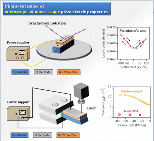
(K,Na)NbO3 (KNN) thin films are promising lead-free piezoelectric materials for microelectromechanical systems (MEMS) devices. However, the origin of the strong piezoelectric properties of KNN thin films remains unclear because crystallographic deformation by piezoelectric effects is not clear in detail. We used synchrotron X-ray diffraction (XRD) to explore the origin of the piezoelectricity of polycrystalline (K0.45Na0.55)NbO3 (KNN) thin films, which led to the observation of large crystal deformation originating from the piezoelectric effects. The peak shifts of the XRD patterns indicated changes in both the out-of-plane and in-plane lattice parameters of KNN. In addition, an electric field-induced phase transition under an applied electric field was observed. The microscopic piezoelectric coefficients (e31,f) were estimated from the in situ XRD results and subsequently compared with the macroscopic piezoelectric coefficients estimated from the converse piezoelectric effect by the cantilever method. The macroscopic |e31,f| coefficients based on the converse piezoelectric effect were in the range of 6.3–11.1 C/m2, whereas the microscopic |e31,f| values based on the in situ XRD results were in the range of 1.2–1.5 C/m2. However, the macroscopic piezoelectric coefficients from the direct piezoelectric effect were 1.6–2.0 C/m2, which were similar to those obtained from the in situ XRD results. The results suggest that the large macroscopic piezoelectric properties associated with the converse piezoelectric effect arise from the observed electric field-induced phase transition. This study demonstrates the main factors associated with the macroscopic piezoelectric properties in lead-free KNN thin films.
中文翻译:

压电(K,Na)NbO 3薄膜的晶体形变原位X射线衍射观察
(K,Na)NbO 3(KNN)薄膜是用于微机电系统(MEMS)器件的有前途的无铅压电材料。但是,KNN薄膜的强压电特性的起源仍然不清楚,因为尚不清楚压电效应引起的晶体变形。我们使用同步加速器X射线衍射(XRD)探索了多晶(K 0.45 Na 0.55)NbO 3的压电性起源(KNN)薄膜,导致观察到源自压电效应的大晶体变形。XRD图谱的峰位移表明KNN的面外和面内晶格参数都发生了变化。另外,观察到在外加电场下电场诱导的相变。根据原位XRD结果估算微观压电系数(e 31,f),然后将其与通过悬臂法根据逆压电效应估算的宏观压电系数进行比较。宏观| e 31,f | 基于逆压电效应的系数在6.3-11.1 C / m 2的范围内,而微观| e 31,f | 根据原位XRD结果得出的数值在1.2–1.5 C / m 2的范围内。然而,直接压电效应产生的宏观压电系数为1.6–2.0 C / m 2,与从原位XRD结果获得的相似。结果表明,与逆压电效应相关的大的宏观压电特性是由观察到的电场诱导的相变产生的。这项研究证明了与无铅KNN薄膜的宏观压电性能有关的主要因素。
更新日期:2020-07-28
中文翻译:
压电(K,Na)NbO 3薄膜的晶体形变原位X射线衍射观察
(K,Na)NbO 3(KNN)薄膜是用于微机电系统(MEMS)器件的有前途的无铅压电材料。但是,KNN薄膜的强压电特性的起源仍然不清楚,因为尚不清楚压电效应引起的晶体变形。我们使用同步加速器X射线衍射(XRD)探索了多晶(K 0.45 Na 0.55)NbO 3的压电性起源(KNN)薄膜,导致观察到源自压电效应的大晶体变形。XRD图谱的峰位移表明KNN的面外和面内晶格参数都发生了变化。另外,观察到在外加电场下电场诱导的相变。根据原位XRD结果估算微观压电系数(e 31,f),然后将其与通过悬臂法根据逆压电效应估算的宏观压电系数进行比较。宏观| e 31,f | 基于逆压电效应的系数在6.3-11.1 C / m 2的范围内,而微观| e 31,f | 根据原位XRD结果得出的数值在1.2–1.5 C / m 2的范围内。然而,直接压电效应产生的宏观压电系数为1.6–2.0 C / m 2,与从原位XRD结果获得的相似。结果表明,与逆压电效应相关的大的宏观压电特性是由观察到的电场诱导的相变产生的。这项研究证明了与无铅KNN薄膜的宏观压电性能有关的主要因素。


 京公网安备 11010802027423号