当前位置:
X-MOL 学术
›
Phys. Status Solidi A
›
论文详情
Our official English website, www.x-mol.net, welcomes your
feedback! (Note: you will need to create a separate account there.)
Informative Aspects of Molten KOH Etch Pits Formed at Basal Plane Dislocations on the Surface of 4H‐SiC
Physica Status Solidi (A) - Applications and Materials Science Pub Date : 2020-07-02 , DOI: 10.1002/pssa.202000332 Johji Nishio 1 , Chiharu Ota 1 , Aoi Okada 1 , Ryosuke Iijima 1
Physica Status Solidi (A) - Applications and Materials Science Pub Date : 2020-07-02 , DOI: 10.1002/pssa.202000332 Johji Nishio 1 , Chiharu Ota 1 , Aoi Okada 1 , Ryosuke Iijima 1
Affiliation
|
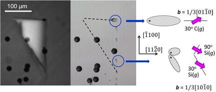
Despite being a destructive technique, molten KOH etch pits at basal plane dislocations are found to have informative aspects, as revealed by photoluminescence imaging and optical microscopy, on the 4° off‐cut (0001) surface of 4H‐SiC p–i–n diode chips, where single Shockley‐type stacking faults have expanded during electroluminescence experiments. Smaller etch pits are observed aligning on single lines along ±[ 100] that are the shallowest sides of stacking faults. Through closer observation of the pits, the facing directions are found to agree well with a model explaining the two types of partial dislocations constituting the line. Other basal plane dislocation pits are observed by scanning electron microscopy on the sublimation‐grown wafer surface before epitaxial growth. The distances between the partial dislocation cores are measured at each pit. No basal plane dislocation etch pit facing toward ±[ 100] is found, but a weak correlation is noted between the partial dislocation distance at the cores and the direction that the basal plane dislocations face. The corresponding results are discussed in terms of the image force and the force exerted on steps perpendicular to the (0001) plane, to understand the mechanisms of basal plane dislocation propagation and/or conversion to threading edge dislocations.
中文翻译:

4H-SiC表面基底平面位错上形成的熔融KOH蚀刻坑的信息性方面
尽管是一种破坏性技术,但发现基面位错处的熔融KOH蚀刻坑在4H‐SiC p–i–n的4°切角(0001)表面上具有有益的方面,如光致发光成像和光学显微镜所揭示的那样。二极管芯片,其中单个Shockley型堆叠故障在电致发光实验中已经扩大。观察到较小的蚀刻坑沿±[100]是堆垛层错最浅的一面。通过对凹坑的仔细观察,发现其朝向与解释构成线的两种类型的部分位错的模型非常吻合。在外延生长之前,通过升华生长的晶片表面的扫描电子显微镜观察到其他基面位错坑。在每个凹坑处测量部分位错核心之间的距离。没有基面错位蚀刻坑面向±[[100]被发现,但是在核心处的部分位错距离与基面位错面对的方向之间发现了弱的相关性。根据图像力和垂直于(0001)平面的台阶上施加的力来讨论相应的结果,以了解基面位错传播和/或转换为螺纹边缘位错的机理。
更新日期:2020-08-24
中文翻译:
4H-SiC表面基底平面位错上形成的熔融KOH蚀刻坑的信息性方面
尽管是一种破坏性技术,但发现基面位错处的熔融KOH蚀刻坑在4H‐SiC p–i–n的4°切角(0001)表面上具有有益的方面,如光致发光成像和光学显微镜所揭示的那样。二极管芯片,其中单个Shockley型堆叠故障在电致发光实验中已经扩大。观察到较小的蚀刻坑沿±[100]是堆垛层错最浅的一面。通过对凹坑的仔细观察,发现其朝向与解释构成线的两种类型的部分位错的模型非常吻合。在外延生长之前,通过升华生长的晶片表面的扫描电子显微镜观察到其他基面位错坑。在每个凹坑处测量部分位错核心之间的距离。没有基面错位蚀刻坑面向±[[100]被发现,但是在核心处的部分位错距离与基面位错面对的方向之间发现了弱的相关性。根据图像力和垂直于(0001)平面的台阶上施加的力来讨论相应的结果,以了解基面位错传播和/或转换为螺纹边缘位错的机理。


 京公网安备 11010802027423号