Nano Energy ( IF 16.8 ) Pub Date : 2020-07-03 , DOI: 10.1016/j.nanoen.2020.104991 Monika Nehra , Neeraj Dilbaghi , Giovanna Marrazza , Ajeet Kaushik , Reza Abolhassani , Yogendra Kumar Mishra , Ki Hyun Kim , Sandeep Kumar
|
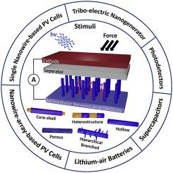
The accomplishment of 1D semiconductor nanowires (SN) in the field of energy has attracted intense interest in recent years due to their advantageous properties (e.g., large surface area, unique surface chemistry, and tunable transport properties). Considerable efforts were devoted to explore 1D-SN building blocks as the harvesting channel/unit (e.g., in thermal, chemical, mechanical, and solar energy applications) and as the storage media (for electrochemical energy). A wide bandgap tuning of SN in the range of 0.39 eV (in case of InAs nanowires) to 4.66 eV (in case of β-Ga2O3 nanowires) due to quantum size effect makes them a suitable candidate for optoelectronic applications. This review focuses on 1D-SN wherein the travel of electron and photon is confined in two directions but in one dimension. The SN emerged as promising nanostructures for developing electronic devices of high carrier-mobilities (e.g., >12000 cm2V−1s−1 for holes and 3000 cm2V−1s−1 for electrons in case of Ge nanowires). A list of efficient fabrication strategies (e.g., vapor-liquid-solid [VLS], hard-template approaches, and solution-phase) are discussed along with ultrafast electron transport dynamics of SN and piezoelectric nanowires. The control on electrons, photons, and phonons transport makes 1D-SN ideal for solid-state energy conversion, harvesting, and storage applications. State-of-the-art 1D-SN energy nano-systems have been demonstrated to yield diverse outcomes of high significance including single-nanowire and array-based photovoltaic cells (InP nanowires with a maximum power conversion efficiency up to 17.8%), nanogenerators (SiGe nanowires with a maximum power output of 7.1 μW/cm2), supercapacitors (core-shell hierarchical CoS@MoS2 nanowire array with an energy density of 95.7 Wh kg−1 at power density of 711.2 W kg−1), and lithium-air batteries (3D freestanding hierarchical CuCo2O4 nanowires@Ni foam with an excellent specific capacity of 13654 mAh g−1 at 0.1 mA cm−2). This review will serve as a key platform to understand 1D-SN to fabricate the next-generation novel nano-systems for developing efficient energy devices of high performance.
中文翻译:
一维半导体纳米线,用于能量转换,收集和存储应用
一维半导体纳米线(SN)在能源领域的成就,近年来由于其优越的性能(例如,大表面积,独特的表面化学性质和可调的传输性能)而引起了人们的极大兴趣。投入了大量的精力来探索1D-SN构建块,作为收获渠道/单位(例如,在热,化学,机械和太阳能应用中)和作为存储介质(用于电化学能)。SN的宽能带隙调谐在0.39电子伏特(在纳米线的InAs的情况下)的范围内,以4.66电子伏特(在以下情况下的β-Ga 2 ö 3纳米线)由于量子尺寸效应而使其成为光电应用的合适候选者。这篇综述着重于一维SN,其中电子和光子的传播被限制在两个方向上,但在一维上。SN作为用于开发高载流子迁移率(例如,> 12000 cm 2 V -1 s -1用于孔和3000 cm 2 V -1 s -1)的高载流子迁移率的电子器件的有前途的纳米结构而出现。对于电子(如Ge纳米线)。与SN和压电纳米线的超快电子传输动力学一起,讨论了一系列有效的制造策略(例如,气液固[VLS],硬模板方法和固溶相)。对电子,光子和声子传输的控制使1D-SN非常适合固态能量转换,收集和存储应用。先进的1D-SN能量纳米系统已被证明具有多种重要意义,包括单纳米线和基于阵列的光伏电池(InP纳米线,其最大功率转换效率高达17.8%),纳米发电机(最大功率输出为7.1μW/ cm 2的SiGe纳米线),超级电容器(核-壳分层CoS @ MoS 2纳米线阵列用95.7瓦千克的能量密度-1在711.2功率密度钨千克-1),和锂-空气电池(3D独立分层CUCO 2个ö 4纳米线@镍泡沫的13654毫安g的优异的比容量-在0.1 mA cm -2时为1)。这篇综述将作为了解1D-SN的关键平台,以制造下一代新型纳米系统,用于开发高性能的高效能源设备。


 京公网安备 11010802027423号