当前位置:
X-MOL 学术
›
ACS Photonics
›
论文详情
Our official English website, www.x-mol.net, welcomes your
feedback! (Note: you will need to create a separate account there.)
Plasmon-Driven Hot Electron Transfer at Atomically Sharp Metal-Semiconductor Nanojunctions.
ACS Photonics ( IF 6.5 ) Pub Date : 2020-06-30 , DOI: 10.1021/acsphotonics.0c00557 Masiar Sistani 1 , Maximilian G Bartmann 1 , Nicholas A Güsken 2 , Rupert F Oulton 2 , Hamid Keshmiri 1 , Minh Anh Luong 3 , Zahra Sadre Momtaz 4 , Martien I Den Hertog 4 , Alois Lugstein 1
ACS Photonics ( IF 6.5 ) Pub Date : 2020-06-30 , DOI: 10.1021/acsphotonics.0c00557 Masiar Sistani 1 , Maximilian G Bartmann 1 , Nicholas A Güsken 2 , Rupert F Oulton 2 , Hamid Keshmiri 1 , Minh Anh Luong 3 , Zahra Sadre Momtaz 4 , Martien I Den Hertog 4 , Alois Lugstein 1
Affiliation
|
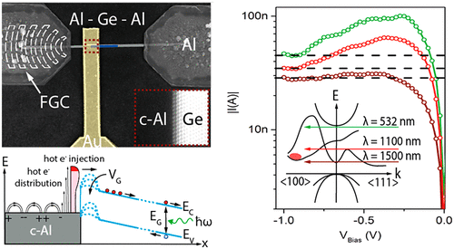
Recent advances in guiding and localizing light at the nanoscale exposed the enormous potential of ultrascaled plasmonic devices. In this context, the decay of surface plasmons to hot carriers triggers a variety of applications in boosting the efficiency of energy-harvesting, photocatalysis, and photodetection. However, a detailed understanding of plasmonic hot carrier generation and, particularly, the transfer at metal–semiconductor interfaces is still elusive. In this paper, we introduce a monolithic metal–semiconductor (Al–Ge) heterostructure device, providing a platform to examine surface plasmon decay and hot electron transfer at an atomically sharp Schottky nanojunction. The gated metal–semiconductor heterojunction device features electrostatic control of the Schottky barrier height at the Al–Ge interface, enabling hot electron filtering. The ability of momentum matching and to control the energy distribution of plasmon-driven hot electron injection is demonstrated by controlling the interband electron transfer in Ge, leading to negative differential resistance.
中文翻译:

等离子尖锐的金属-半导体纳米结处的等离子体驱动热电子转移。
在纳米级引导和定位光的最新进展暴露了超规模等离子体设备的巨大潜力。在这种情况下,表面等离子体激元衰减为热载流子会触发各种应用,以提高能量收集,光催化和光检测的效率。但是,对等离子热载流子产生,尤其是金属-半导体界面上的转移的详细了解仍然难以捉摸。在本文中,我们介绍了一种单片金属-半导体(Al-Ge)异质结构器件,提供了一个在原子尖锐的肖特基纳米结处检查表面等离子体激元衰减和热电子传递的平台。栅金属-半导体异质结器件具有对Al-Ge界面处的肖特基势垒高度进行静电控制的功能,从而可以进行热电子滤波。
更新日期:2020-07-15
中文翻译:
等离子尖锐的金属-半导体纳米结处的等离子体驱动热电子转移。
在纳米级引导和定位光的最新进展暴露了超规模等离子体设备的巨大潜力。在这种情况下,表面等离子体激元衰减为热载流子会触发各种应用,以提高能量收集,光催化和光检测的效率。但是,对等离子热载流子产生,尤其是金属-半导体界面上的转移的详细了解仍然难以捉摸。在本文中,我们介绍了一种单片金属-半导体(Al-Ge)异质结构器件,提供了一个在原子尖锐的肖特基纳米结处检查表面等离子体激元衰减和热电子传递的平台。栅金属-半导体异质结器件具有对Al-Ge界面处的肖特基势垒高度进行静电控制的功能,从而可以进行热电子滤波。


 京公网安备 11010802027423号