Our official English website, www.x-mol.net, welcomes your feedback! (Note: you will need to create a separate account there.)
Ultrafast and Sensitive Self-Powered Photodetector Featuring Self-Limited Depletion Region and Fully Depleted Channel with van der Waals Contacts.
ACS Nano ( IF 17.1 ) Pub Date : 2020-06-30 , DOI: 10.1021/acsnano.0c04329 Mingjin Dai , Hongyu Chen , Fakun Wang 1 , Mingsheng Long 2 , Huiming Shang , Yunxia Hu , Wen Li , Chuanyang Ge , Jia Zhang , Tianyou Zhai 1 , Yongqing Fu 3 , PingAn Hu
ACS Nano ( IF 17.1 ) Pub Date : 2020-06-30 , DOI: 10.1021/acsnano.0c04329 Mingjin Dai , Hongyu Chen , Fakun Wang 1 , Mingsheng Long 2 , Huiming Shang , Yunxia Hu , Wen Li , Chuanyang Ge , Jia Zhang , Tianyou Zhai 1 , Yongqing Fu 3 , PingAn Hu
Affiliation
|
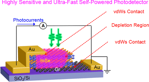
Self-powered photodetectors with great potential for implanted medical diagnosis and smart communications have been severely hindered by the difficulty of simultaneously achieving high sensitivity and fast response speed. Here, we report an ultrafast and highly sensitive self-powered photodetector based on two-dimensional (2D) InSe, which is achieved by applying a device architecture design and generating ideal Schottky or ohmic contacts on 2D layered semiconductors, which are difficult to realize in the conventional semiconductors owing to their surface Fermi-level pinning. The as-fabricated InSe photodiode features a maximal lateral self-limited depletion region and a vertical fully depleted channel. It exhibits a high detectivity of 1.26 × 10¹³ Jones and an ultrafast response speed of ∼200 ns, which breaks the response speed limit of reported self-powered photodetectors based on 2D semiconductors. The high sensitivity is achieved by an ultralow dark current noise generated from the robust van der Waals (vdW) Schottky junction and a high photoresponsivity due to the formation of a maximal lateral self-limited depletion region. The ultrafast response time is dominated by the fast carrier drift driven by a strong built-in electric field in the vertical fully depleted channel. This device architecture can help us to design high-performance photodetectors utilizing vdW layered semiconductors.
中文翻译:

超快灵敏的自供电光电探测器,具有自限耗尽区和完全耗尽的通道,具有范德华触点。
同时实现高灵敏度和快速响应速度的困难严重阻碍了具有强大潜力的自供电光电探测器在植入式医学诊断和智能通信中的应用。在这里,我们报告了一种基于二维(2D)InSe的超快速,高灵敏度的自供电光电探测器,该探测器是通过应用器件架构设计并在2D层状半导体上生成理想的肖特基或欧姆接触而实现的,这在半导体中很难实现。传统半导体由于其表面的费米能级钉扎。制成的InSe光电二极管具有最大的横向自限耗尽区和垂直的完全耗尽通道。它显示出1.26×10 13的高检测率Jones和约200 ns的超快响应速度,打破了报道的基于2D半导体的自供电光电探测器的响应速度极限。高灵敏度是通过鲁棒的范德华(vdW)肖特基结产生的超低暗电流噪声以及由于形成最大的横向自限耗尽区而产生的高光响应性来实现的。超快响应时间主要由垂直完全耗尽通道中强大的内置电场驱动的快速载流子漂移决定。这种器件架构可以帮助我们设计使用vdW分层半导体的高性能光电探测器。
更新日期:2020-07-28
中文翻译:
超快灵敏的自供电光电探测器,具有自限耗尽区和完全耗尽的通道,具有范德华触点。
同时实现高灵敏度和快速响应速度的困难严重阻碍了具有强大潜力的自供电光电探测器在植入式医学诊断和智能通信中的应用。在这里,我们报告了一种基于二维(2D)InSe的超快速,高灵敏度的自供电光电探测器,该探测器是通过应用器件架构设计并在2D层状半导体上生成理想的肖特基或欧姆接触而实现的,这在半导体中很难实现。传统半导体由于其表面的费米能级钉扎。制成的InSe光电二极管具有最大的横向自限耗尽区和垂直的完全耗尽通道。它显示出1.26×10 13的高检测率Jones和约200 ns的超快响应速度,打破了报道的基于2D半导体的自供电光电探测器的响应速度极限。高灵敏度是通过鲁棒的范德华(vdW)肖特基结产生的超低暗电流噪声以及由于形成最大的横向自限耗尽区而产生的高光响应性来实现的。超快响应时间主要由垂直完全耗尽通道中强大的内置电场驱动的快速载流子漂移决定。这种器件架构可以帮助我们设计使用vdW分层半导体的高性能光电探测器。


 京公网安备 11010802027423号